IS42S32400D
Integrated Silicon Solution, Inc. — www.issi.com
19
Rev. F
03/03/09
FUNCTIONAL DESCRIPTION
The 128Mb SDRAMs are quad-bank DRAMs which operate
at 3.3V and include a synchronous interface (all signals are
registered on the positive edge of the clock signal, CLK).
Each of the 33,554,432-bit banks is organized as 4,096
rows by 256 columns by 32 bits.
Read and write accesses to the SDRAM are burst oriented;
accesses start at a selected location and continue for a
programmed number of locations in a programmed
sequence. Accesses begin with the registration of an AC-
TIVE command which is then followed by a READ or WRITE
command. The address bits registered coincident with the
ACTIVE command are used to select the bank and row to
be accessed
(BA0 and BA1 select the bank, A0-A11 select the row)
.
The address bits
A0-A7
registered coincident with the READ
or WRITE command are used to select the starting column
location for the burst access.
Prior to normal operation, the SDRAM must be initialized.
The following sections provide detailed information covering
device initialization, register definition, command
descriptions and device operation.
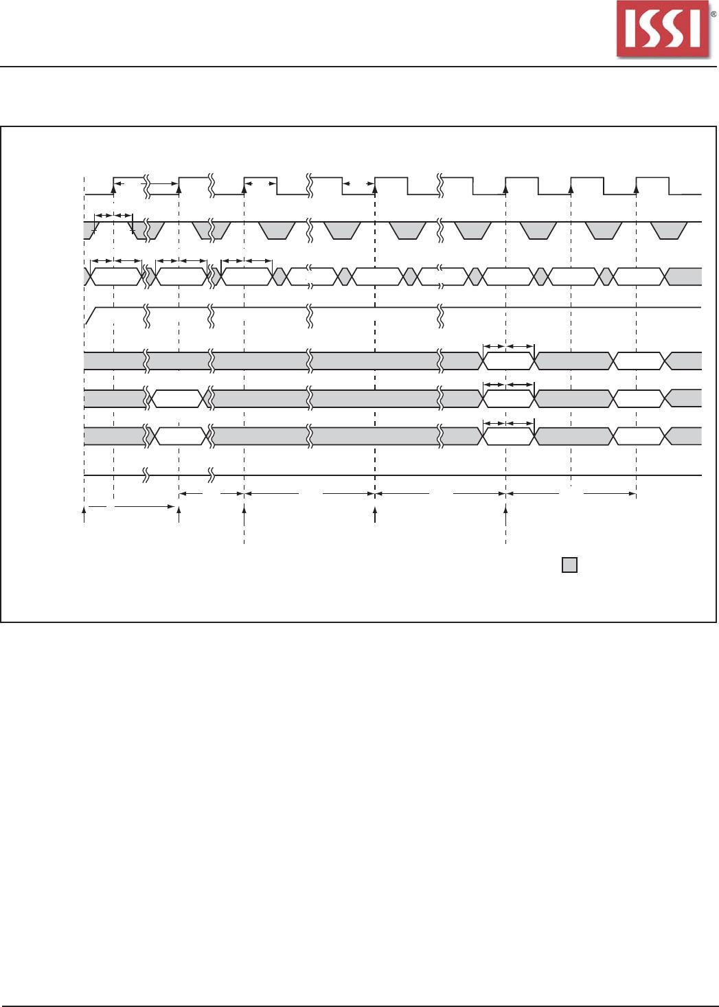
Initialization
SDRAMs must be powered up and initialized in a
predefined manner.
The 128M SDRAM is initialized after the power is applied to
VDD and VDDQ (simultaneously) and the clock is stable with
DQM High and CKE High.
A 100µs delay is required prior to issuing any command
other than a
COMMAND INHIBIT
or a
NOP
. The COMMAND
INHIBIT or NOP may be applied during the 100µs period and
should continue at least through the end of the period.
With at least one COMMAND INHIBIT or NOP command
having been applied, a PRECHARGE command should be
applied once the 100µs delay has been satisfied. All banks
must be precharged. This will leave all banks in an idle state
after which at least two
AUTO REFRESH
cycles must be
performed. After the
AUTO REFRESH
cycles are complete,
the SDRAM is then ready for mode register programming.
The mode register should be loaded prior to applying any
operational command because it will power up in an un-
known state.