22
Integrated Silicon Solution, Inc. — www.issi.com
Rev. F
03/03/09
IS42S32400D
SELF-REFRESH CYCLE
CLK
CKE
COMMAND
DQM0 - DQM3
A0-A9, A11
A10
BA0, BA1
DQ
t
AS
t
AH
BANK
t
CL
t
CH
t
CK
t
CMS
t
CMH
t
CKS
t
CKH
ALL BANKS
SINGLE BANK
t
CKS
Precharge all
active banks
CLK stable prior to exiting
self refresh mode
Enter self
refresh
mode
Exit
self refresh
mode
(Restart refresh time base)
T0 T1 T2 Tn+1 To+1 To+2
High-Z
Auto
Refresh
Auto
Refresh
PRECHARGE
NOP NOP NOP
t
CKS
tRAS
tRP
tXSR
DON'T CARE
IS42S32400D
Integrated Silicon Solution, Inc. — www.issi.com
23
Rev. F
03/03/09
REGISTER DEFINITION
Mode Register
The mode register is used to define the specific mode of
operation of the SDRAM. This definition includes the
selection of a burst length, a burst type, a CAS latency, an
operating mode and a write burst mode, as shown in MODE
REGISTER DEFINITION.
The mode register is programmed via the LOAD MODE
REGISTER command and will retain the stored information
until it is programmed again or the device loses power.
Mode register bits M0-M2 specify the burst length, M3
specifies the type of burst
(sequential or interleaved)
, M4- M6
specify the CAS latency, M7 and M8 specify the operating
mode, M9 specifies the WRITE burst mode, and M10 and
M11 are reserved for future use.
The mode register must be loaded when all banks are idle,
and the controller must wait the specified time before
initiating the subsequent operation. Violating either of these
requirements will result in unspecified operation.
MODE REGISTER DEFINITION
Latency Mode
M6 M5 M4 CAS Latency
0 0 0 Reserved
0 0 1 Reserved
0 1 0 2
0 1 1 3
1 0 0 Reserved
1 0 1 Reserved
1 1 0 Reserved
1 1 1 Reserved
1. To ensure compatibility with future devices,
should program BA1, BA0, A11, A10 = "0"
Write Burst Mode
M9 Mode
0 Programmed Burst Length
1 Single Location Access
Operating Mode
M8 M7 M6-M0 Mode
0 0 Defined Standard Operation
All Other States Reserved
Burst Type
M3 Type
0 Sequential
1 Interleaved
Burst Length
M2 M1 M0 M3=0 M3=1
0 0 0 1 1
0 0 1 2 2
0 1 0 4 4
0 1 1 8 8
1 0 0 Reserved Reserved
1 0 1 Reserved Reserved
1 1 0 Reserved Reserved
1 1 1 Full Page Reserved
Reserved
Address Bus
Mode Register (Mx)
(1)
BA1 BA0
A11 A10 A9 A8 A7 A6 A5 A4 A3 A2 A1 A0
24
Integrated Silicon Solution, Inc. — www.issi.com
Rev. F
03/03/09
IS42S32400D
BURST DEFINITION
Burst Starting Column Order of Accesses Within a Burst
Length Address Type = Sequential Type = Interleaved
A0
2 0 0-1 0-1
1 1-0 1-0
A1 A0
0 0 0-1-2-3 0-1-2-3
4 0 1 1-2-3-0 1-0-3-2
1 0 2-3-0-1 2-3-0-1
1 1 3-0-1-2 3-2-1-0
A2 A1 A0
0 0 0 0-1-2-3-4-5-6-7 0-1-2-3-4-5-6-7
0 0 1 1-2-3-4-5-6-7-0 1-0-3-2-5-4-7-6
0 1 0 2-3-4-5-6-7-0-1 2-3-0-1-6-7-4-5
8 0 1 1 3-4-5-6-7-0-1-2 3-2-1-0-7-6-5-4
1 0 0 4-5-6-7-0-1-2-3 4-5-6-7-0-1-2-3
1 0 1 5-6-7-0-1-2-3-4 5-4-7-6-1-0-3-2
1 1 0 6-7-0-1-2-3-4-5 6-7-4-5-2-3-0-1
1 1 1 7-0-1-2-3-4-5-6 7-6-5-4-3-2-1-0
Full n = A0-A7 Cn, Cn + 1, Cn + 2 Not Supported
Page Cn + 3, Cn + 4...
(y) (location 0-y) …Cn - 1,
Cn…
BURST LENGTH
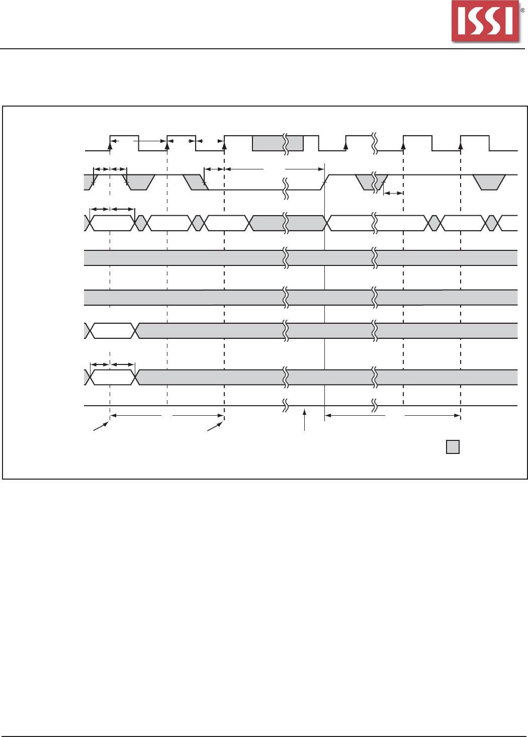
Read and write accesses to the SDRAM are burst oriented,
with the burst length being programmable, as shown in
MODE REGISTER DEFINITION. The burst length deter-
mines the maximum number of column locations that can
be accessed for a given READ or WRITE command. Burst
lengths of 1, 2, 4 or 8 locations are available for both the
sequential and the interleaved burst types, and a full-page
burst is available for the sequential type. The full-page burst
is used in conjunction with the BURST TERMINATE com-
mand to generate arbitrary burst lengths.
Reserved states should not be used, as unknown operation
or incompatibility with future versions may result.
When a READ or WRITE command is issued, a block of
columns equal to the burst length is effectively selected. All
accesses for that burst take place within this block, mean-
ing that the burst will wrap within the block if a boundary is
reached. The block is uniquely selected by A1-A7 (x32)
when the burst length is set to two; by A2-A7 (x32) when the
burst length is set to four; and by A3-A7 (x32) when the burst
length is set to eight. The remaining (least significant)
address bit(s) is (are) used to select the starting location
within the block. Full-page bursts wrap within the page if the
boundary is reached.
Burst Type
Accesses within a given burst may be programmed to be
either sequential or interleaved; this is referred to as the
burst type and is selected via bit M3.
The ordering of accesses within a burst is determined by the
burst length, the burst type and the starting column address,
as shown in BURST DEFINITION table.

IS42S32400D-7T-TR

Mfr. #:
Manufacturer:
Description:
IC DRAM 128M PARALLEL 86TSOP II
Lifecycle:
New from this manufacturer.
Delivery:
DHL FedEx Ups TNT EMS
Payment:
T/T Paypal Visa MoneyGram Western Union