28
Integrated Silicon Solution, Inc. — www.issi.com
Rev. F
03/03/09
IS42S32400D
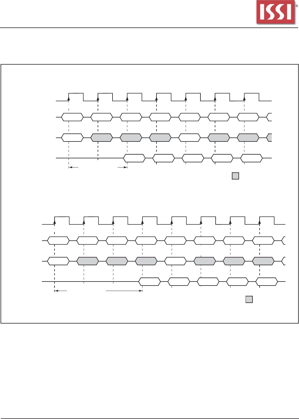
possible CAS latency; data element
n
+ 3 is either the last of
a burst of four or the last desired of a longer burst. Following
the PRECHARGE command, a subsequent command to the
same bank cannot be issued until tRP is met. Note that part
of the row precharge time is hidden during the access of the
last data element(s).
In the case of a fixed-length burst being executed to
completion, a PRECHARGE command issued at the opti-
mum time (as described above) provides the same opera-
tion that would result from the same fixed-length burst with
auto precharge. The disadvantage of the PRECHARGE
command is that it requires that the command and address
buses be available at the appropriate time to issue the
command; the advantage of the PRECHARGE command is
that it can be used to truncate fixed-length or full-page
bursts.
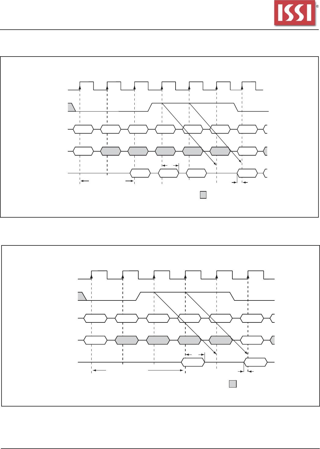
Full-page READ bursts can be truncated with the BURST
TERMINATE command, and fixed-length READ bursts
may be truncated with a BURST TERMINATE command,
provided that auto precharge was not activated. The BURST
TERMINATE command should be issued
x
cycles before
the clock edge at which the last desired data element is
valid, where
x
equals the CAS latency minus one. This is
shown in the READ Burst Termination diagram for each
possible CAS latency; data element
n
+ 3 is the last desired
data element of a longer burst.