IS42S32400D
Integrated Silicon Solution, Inc. — www.issi.com
37
Rev. F
03/03/09
CLK
CKE
HIGH
COLUMN ADDRESS
AUTO PRECHARGE
BANK ADDRESS
CS
RAS
CAS
WE
A0-A7
A10
BA0, BA1
NO PRECHARGE
A8, A9, A11
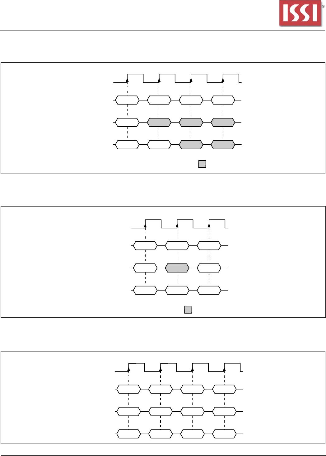
WRITE COMMAND
The starting column and bank addresses are provided with
the WRITE command, and auto precharge is either enabled
or disabled for that access. If auto precharge is enabled, the
row being accessed is precharged at the completion of the
burst. For the generic WRITE commands used in the
following illustrations, auto precharge is disabled.
During WRITE bursts, the first valid
data-in
element will be
registered coincident
with the
WRITE
command.
Subsequent
data elements will be registered on each successive positive
clock edge. Upon completion of a fixed-length burst, assum-
ing no other commands have been initiated, the DQs will
remain High-Z and any additional input data will be ignored
(see WRITE Burst). A full-page burst will continue until
terminated. (At the end of the page, it will wrap to column 0
and continue.)
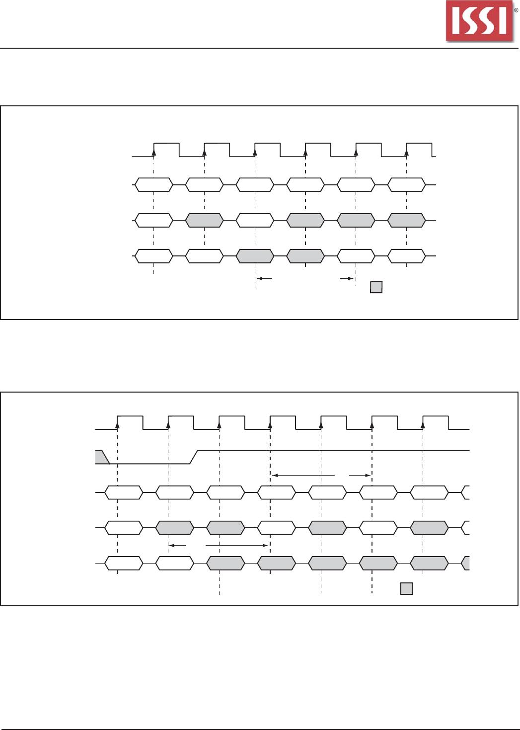
Data for any WRITE burst may be truncated with a subse-
quent WRITE command, and data for a fixed-length WRITE
burst may be immediately followed by data for a WRITE
command. The new WRITE command can be issued on any
clock following the previous WRITE command, and the data
provided coincident with the new command applies to the new
command.
An example is shown in WRITE to WRITE diagram. Data
n
+ 1 is either the last of a burst of two or the last desired of
a longer burst. The 128Mb SDRAM uses a pipelined
architecture and therefore does not require the
2n
rule
associated with a prefetch architecture. A WRITE command
can be initiated on any clock cycle following a previous
WRITE command. Full-speed random write accesses within
a page can be performed to the same bank, as shown in
Random WRITE Cycles, or each subsequent WRITE may
be performed to a different bank.
Data for any WRITE burst may be truncated with a subse-
quent READ command, and data for a fixed-length WRITE
burst may be immediately followed by a subsequent READ
command. Once the READ com mand is registered, the
data inputs will be ignored, and WRITEs will not be ex-
ecuted. An example is shown in WRITE to READ. Data
n
+
1 is either the last of a burst of two or the last desired of a
longer burst.
Data for a fixed-length WRITE burst may be followed by, or
truncated with, a PRECHARGE command to the same bank
(provided that auto precharge was not activated), and a full-
page WRITE burst may be truncated with a PRECHARGE
command to the same bank. The PRECHARGE command
should be issued tDPL after the clock edge at which the last
desired input data element is registered. The auto precharge
mode requires a tDPL of at least one clock plus time,
regardless of frequency. In addition, when truncating a
WRITE burst, the DQM signal must be used to mask input
data for the clock edge prior to, and the clock edge coincident
with, the PRECHARGE command. An example is shown in the
WRITE to PRECHARGE diagram. Data
n
+1 is either the last
of a burst of two or the last desired of a longer burst. Following
the PRECHARGE command, a subsequent command to the
same bank cannot be issued until tRP is met.
In the case of a fixed-length burst being executed to comple-
tion, a PRECHARGE command issued at the optimum time
(as
described above)
provides the same operation that would result
from the same fixed-length burst with auto precharge. The
disadvantage of the
PRECHARGE
command is that it requires
that the command and address buses be available at the
appropriate time to issue the command; the advantage of the
PRECHARGE command is that it can be used to truncate
fixed-length or full-page bursts.
Fixed-length or full-page WRITE bursts can be truncated
with the BURST TERMINATE command. When truncating
a WRITE burst, the input data applied coincident with the
BURST TERMINATE command will be ignored. The last
data written (provided that DQM is LOW at that time) will be
the input data applied one clock previous to the BURST
TERMINATE command. This is shown in WRITE Burst
Termination, where data
n
is the last desired data element
of a longer burst.
WRITES
WRITE bursts are initiated with a WRITE command, as
shown in WRITE Command diagram.