VS-VSKT250-08PBF

VS-VSK.170PbF, VS-VSK.250PbF Series
www.vishay.com
Vishay Semiconductors
Revision: 09-Feb-17
4
Document Number: 94417
For technical questions within your region: DiodesAmericas@vishay.com
, DiodesAsia@vishay.com, DiodesEurope@vishay.com
THIS DOCUMENT IS SUBJECT TO CHANGE WITHOUT NOTICE. THE PRODUCTS DESCRIBED HEREIN AND THIS DOCUMENT
ARE SUBJECT TO SPECIFIC DISCLAIMERS, SET FORTH AT www.vishay.com/doc?91000
Note
Table shows the increment of thermal resistance R
thJC
when devices operate at different conduction angles than DC
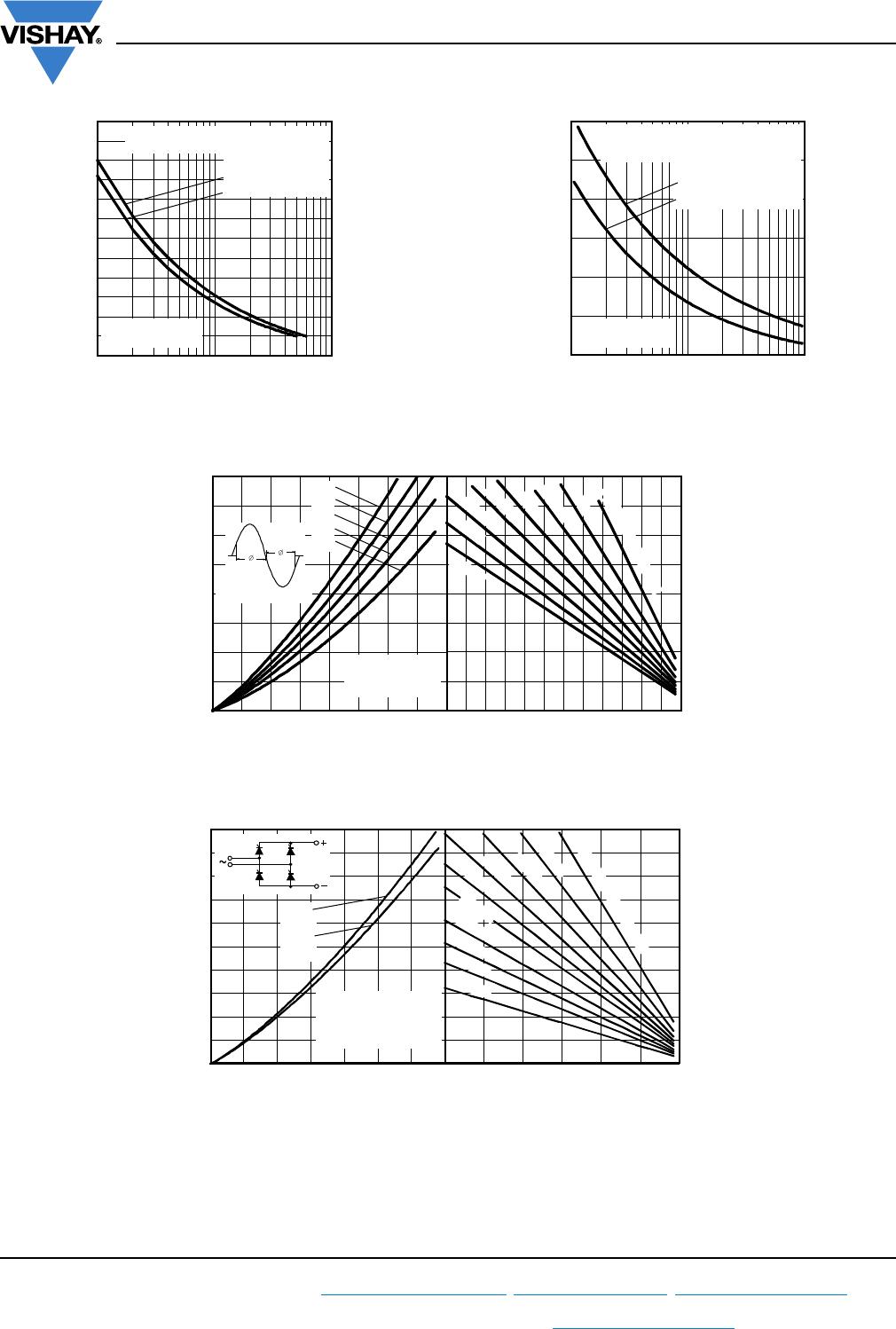
Fig. 1 - Current Ratings Characteristics
Fig. 2 - Current Ratings Characteristics
Fig. 3 - On-State Power Loss Characteristics
Fig. 4 - On-State Power Loss Characteristics
R CONDUCTION PER JUNCTION
DEVICES
SINUSOIDAL CONDUCTION AT T
J
MAXIMUM RECTANGULAR CONDUCTION AT T
J
MAXIMUM
UNITS
180° 120° 90° 60° 30° 180° 120° 90° 60° 30°
VSK.170- 0.009 0.010 0.010 0.020 0.032 0.007 0.011 0.015 0.020 0.033
K/W
VSK.250- 0.009 0.010 0.014 0.020 0.032 0.007 0.011 0.015 0.020 0.033
60
70
80
90
100
110
120
130
0 40 80 120 160 200
30°
60°
90°
120°
180°
Average On-state Current (A)
Maximum Allowable Case Temperature (°C)
Conduction Angle
VSK.170.. series
R
thJC
(DC) = 0.17 K/W
60
70
80
90
100
110
120
130
0 50 100 150 200 250 3
00
DC
30°
60°
90°
120°
180°
Average On-state Current (A)
Maximum Allowable Case Temperature (°C)
Conduction Period
VSK.170.. series
R
thJC
(DC) = 0.17 K/W
0
50
100
150
200
250
300
040801201602
00
RMS limit
Conduction angle
Maximum Average On-state Power Loss (W)
Average On-state Current (A)
180°
120°
90°
60°
30°
VSK.170.. series
per junction
T
J
= 125° C
0
50
100
150
200
250
300
350
0 50 100 150 200 250 3
00
DC
180°
120°
90°
60°
30°
RMS limit
Conduction period
Maximum Average On-state Power Loss (W)
Average On-state Current (A)
VSK.170.. series
per junction
T
J
= 125°C
VS-VSK.170PbF, VS-VSK.250PbF Series
www.vishay.com
Vishay Semiconductors
Revision: 09-Feb-17
5
Document Number: 94417
For technical questions within your region: DiodesAmericas@vishay.com
, DiodesAsia@vishay.com, DiodesEurope@vishay.com
THIS DOCUMENT IS SUBJECT TO CHANGE WITHOUT NOTICE. THE PRODUCTS DESCRIBED HEREIN AND THIS DOCUMENT
ARE SUBJECT TO SPECIFIC DISCLAIMERS, SET FORTH AT www.vishay.com/doc?91000
Fig. 5 - Maximum Non-Repetitive Surge Current Fig. 6 - Maximum Non-Repetitive Surge Current
Fig. 7 - On-State Power Loss Characteristics
Fig. 8 - On-State Power Loss Characteristics
2000
2500
3000
3500
4000
4500
5000
110100
Number Of Equal Amplitude Half Cycle Current Pulses (N)
At any rated load condition and with
rated V
RRM
applied following surge.
Peak Half Sine Wave On-state Current (A)
VSK.170.. series
per junction
Initial T
J
= 130 °C
at 60 Hz 0.0083 s
at 50 Hz 0.0100 s
2000
2500
3000
3500
4000
4500
5000
0.01 0.1 1
Peak Half Sine Wave On-state Current (A)
Pulse Train Duration (s)
Maximum non-repetitive surge current
vs. pulse train duration. Control of
conduction may not be maintained
.
Initial T
J
= 130 °C
No voltage reapplied
Rated V
RRM
reapplied
VSK.170.. series
per junction
020406080100120
0
.
3
5
K
/
W
0
.
3
K
/
W
0
.
2
5
K
/
W
0
.
2
K
/
W
0
.
0
8
K
/
W
0.
1
2
K
/
W
0
.
1
6
K
/
W
Maximum Allowable Ambient Temperature (°C)
R
=
0
.
0
4
K
/
W
-
D
e
l
t
a
R
t
h
S
A
0
50
100
150
200
250
300
350
400
0 50 100 150 200 250 300 350 400
180°
120°
90°
60°
30°
Maximum Total On-state Power Loss (W)
Total RMS Output Current (A)
Conduction angle
VSK.170.. series
per module
T
J
= 130 °C
0 20406080100120
Maximum Allowable Ambient Temperature (°C)
R
=
0
.
0
2
K
/
W
-
D
e
l
t
a
R
0
.
0
4
K
/
W
t
h
S
A
0
.
0
6
K
/
W
0
.
0
8
K
/
W
0
.
1
K
/
W
0
.1
2
K
/
W
0
.
1
6
K
/
W
0
.
2
K
/
W
0
.
2
5
K
/
W
0
.
3
5
K
/
W
0
100
200
300
400
500
600
700
800
900
1000
0 50 100 150 200 250 300 350
Total Output Current (A)
Maximum Total Power Loss (W)
180°
(sine)
180°
(rect.)
2 x VSK.170.. series
single phase bridge
connected
T
J
= 130 °C
VS-VSK.170PbF, VS-VSK.250PbF Series
www.vishay.com
Vishay Semiconductors
Revision: 09-Feb-17
6
Document Number: 94417
For technical questions within your region: DiodesAmericas@vishay.com
, DiodesAsia@vishay.com, DiodesEurope@vishay.com
THIS DOCUMENT IS SUBJECT TO CHANGE WITHOUT NOTICE. THE PRODUCTS DESCRIBED HEREIN AND THIS DOCUMENT
ARE SUBJECT TO SPECIFIC DISCLAIMERS, SET FORTH AT www.vishay.com/doc?91000
Fig. 9 - On-State Power Loss Characteristics
Fig. 10 - Current Ratings Characteristics
Fig. 11 - Current Ratings Characteristics
Fig. 12 - On-State Power Loss Characteristics
Fig. 13 - On-State Power Loss Characteristics
020406080100120
Maximum Allowable Ambient Temperature (°C)
0
.
2
5
K
/
W
0
.
1
6K
/
W
0
.
1
2
K
/
W
0
.
1
K
/
W
0
.
0
8
K
/
W
0
.
0
5
K
/
W
0
.
0
3
K
/
W
R
=
0
.
0
1
K
/
W
-
D
e
l
t
a
R
t
h
S
A
0
200
400
600
800
1000
1200
1400
1600
0 100 200 300 400 500
Total Output Current (A)
Maximum Total Power Loss (W)
120°
(Rect)
3 x VSK.170.. series
three phase bridge
connected
T
J
= 130 °C
60
70
80
90
100
110
120
130
0 50 100 150 200 250 3
00
30°
60°
90°
120°
180°
Average On-state Current (A)
Maximum Allowable Case Temperature (°C)
Conduction angle
VSK.250.. series
R
thJC
(DC) = 0.125 K/W
60
70
80
90
100
110
120
130
0 100 200 300 400 5
00
DC
30°
60°
90°
120°
180°
Average On-state Current (A)
Maximum Allowable Case Temperature (°C)
Conduction period
VSK.250.. Series
R
thJC
(DC) = 0.125 K/W
0
50
100
150
200
250
300
350
050100150200250
RMS limit
Conduction Angle
Maximum Average On-state Power Loss (W
)
Average On-state Current (A)
180°
120°
90°
60°
30°
VSK.250.. series
per junction
T = 130 °C
J

VS-VSKT250-08PBF

Mfr. #:
Manufacturer:
Vishay Semiconductors
Description:
SCR Modules 800volt 250amp
Lifecycle:
New from this manufacturer.
Delivery:
DHL FedEx Ups TNT EMS
Payment:
T/T Paypal Visa MoneyGram Western Union