LTC2925
10
2925fd
For more information www.linear.com/LTC2925
applicaTions inForMaTion
Tracking Cell
The LTC2925’s operation is based on the tracking cell
shown in Figure 5, which uses a proprietary wide-range
current mirror. The tracking cell shown in Figure 5 servos
the TRACK pin at 0.8V. The current supplied by the TRACK
pin is mirrored at the FB pin to establish a voltage at the
output of the slave supply. The slave output voltage varies
with the master signal, enabling the slave supply to be
controlled as a function of the master signal with terms
set by R
TA
and R
TB
. By selecting appropriate values of
R
TA
and R
TB
, it is possible to generate any of the profiles
in Figures 1 to 4.
In a properly designed system, when the master signal
has reached its maximum voltage the current from the
TRACK1 pin is zero. In this case, there is no current from
the FB1 pin and the LTC2925 has no effect on the output
voltage accuracy, transient response or stability of the
slave supply.
When the ON pin falls below V
ON(TH)
V
ON(HYST)
, typi-
cally 1.225V, the GA
TE pin pulls down with 10µA and the
master signal and the slave supplies will fall at the same
rate as they rose previously.
The ON pin can be controlled by a digital I/O pin or it
can be used to monitor an input supply. By connecting a
resistive divider from an input supply to the ON pin, the
supplies will ramp up only after the monitored supply has
reached a preset voltage.
+
R
TA
R
TB
FB
TRACK
MASTER
0.8V
V
CC
R
FA
2925 F05
SLAVE
R
FB
DC/DC
+
FB OUT
Figure 5. Simplified Tracking Cell
Controlling the Ramp-Up and Ramp-Down Behavior
The operation of the LTC2925 is most easily understood by
referring to the simplified functional diagram in Figure 6.
When the ON pin is low, the GATE pin is pulled to ground
causing the master signal to remain low. Since the current
through R
TB1
is at its maximum when the master signal
is low, the current from FB1 is also at its maximum. This
current drives the slaves output to its minimum voltage.
When the ON pin rises above 1.23V, the master signal rises
and the slave supply tracks the master signal. The ramp
rate is set by an external capacitor driven by a 10µA current
source from an internal charge pump. If no external FET
is used, the ramp rate is set by tying the RAMP and GATE
pins together at one terminal of the external capacitor (see
the Ratiometric Tracking Example).
1.2V
+
+
+
GATE
Q1
MASTER
SLAVE1
C
GATE
1.2V
ON
RAMPBUF
10µA
V
CC
V
CC
R
ONB
R
ONA
R
TA1
R
TB1
10µA
50µA
2µA
RAMP
FB1
TRACK1
0.8V
R
FA1
R
FB1
DC/DC
2925 F06
1×
50mV
SENSEN
SENSEP
SENSEP – SENSEN > 50mV
SCTMR
Figure 6. Simplified Functional Block Diagram
LTC2925
11
2925fd
For more information www.linear.com/LTC2925
Optional External FET
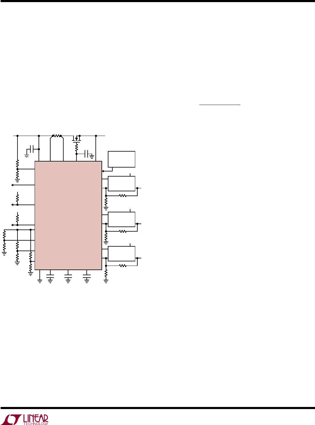
Figure 7 illustrates how an optional external N-channel
FET can ramp up a single supply that becomes the mas
-
ter signal. When used, the FETs gate is tied to the GATE
pin and its source is tied to the RAMP pin. Under normal
operation, the GATE pin sources or sinks 10µA to ramp
the FETs gate up or down at a rate set by the external
capacitor connected to the GATE pin.
The series FET easily controls any supply with an output
voltage between 0V and V
CC
. See the Typical Applications
section for examples.
The short-circuit timer duration is configured by a capaci-
tor tied between SCTMR and GND. SCTMR will pull up
with 50µA when SENSEP
SENSEN > 50mV. Otherwise,
it pulls down with 2µA. When the voltage at SCTMR
exceeds 1.23V, the GATE will be pulled to ground with
20mA and the FAULT pin will be pulled low. Thus, the
capacitor, C
SCTMR
, required to configure the short-circuit
timer duration, t
SCTMR
is determined from:
C
SCTMR
SCTMR
=
Because the slave supplies track the RAMP pin which
is driven by the external FET, they are pulled low by the
tracking circuit when a short-circuit fault occurs. Following
a short-circuit fault, the FET is latched off and FAULT is
pulled low until the fault is cleared by pulling the ON pin
below 0.4V. Note that the supplies will not be allowed to
ramp up again until SCTMR has been pulled below about
100mV by the 2µA pull-down current source. The electronic
circuit breaker supports any supply voltage between 0V
and V
CC
. Although it is normally used to monitor current
through the optional series FET, it is capable of monitoring
other currents, including the current from a slave supply.
The Typical Applications section shows one such example.
If the electronic circuit breaker is not used, tie SENSEP
and SENSEN to V
CC
and SCTMR to GND.
Power Good Timeout
The power good timeout circuit turns off the supplies if an
external supply monitor, connected to the PGI pin, fails to
indicate that all supplies have entered regulation in time
after power up begins. After power up is complete, it turns
off the supplies if any supply exits regulation.
The power good timer duration is configured by a capacitor
tied between PGTMR and GND. PGTMR will pull up the
CPGTMR capacitor with 10µA starting when the ON pin
is driven above 1.23V. Once the voltage at the PGTMR
exceeds 1.23V, a fault will trip if the PGI pin is low. When
the power good timeout circuit detects a fault, the GATE
applicaTions inForMaTion
R
SENSE
Q1
0.1µF
C
PGTMR
10k
V
CC
SENSEP SENSEN
3.3V
V
IN
3.3V
R
ONB
V
IN
R
TB1
R
TB2
R
FA2
2.5V
SLAVE2
MASTER
R
FB2
R
TA2
R
TB3
R
TA3
R
TA1
R
ONA
RAMPBUF
TRACK1
TRACK2
TRACK3
FB2
GATE
LTC2925
PGTMR
C
SDTMR
SDTMR
C
SCTMR
SCTMRGND
2925 F07
RAMP
R
FA3
1.5V
SLAVE3
R
FB3
DC/DC
IN
FB = 0.8V OUT
DC/DC
IN
FB = 0.8V
RUN/SS
RUN/SS
OUT
FB3
3.3V
PGI
R
FA1
1.8V
SLAVE1
R
FB1
SUPPLY
MONITOR
DC/DC
IN
FB = 1.235V
RUN/SS
OUT
FB1
FAULT
ON
10k
V
IN
STATUS
REMOTE
RST
SD3
SD2
SD1
C
GATE
10Ω
Figure 7. Typical Application with External FET
Electronic Circuit Breaker
The LTC2925 features an electronic circuit breaker function
that protects the optional series FET against short circuits.
An external sense resistor is used to measure the current
flowing in the FET. If the voltage across the sense resistor
exceeds 50mV for more than a short-circuit timer cycle,
the gate of the FET is pulled low with 20mA, turning it off.
LTC2925
12
2925fd
For more information www.linear.com/LTC2925
pin is pulled low, the supplies are latched off, and the
FAULT pin is held low until the fault is cleared by taking
the ON pin below 0.4V.
The PGI pin, which is normally connected to the RST pin of
an external supply monitor, is pulled up with 10µA through
a Schottky diode allowing it to be pulled safely above V
CC
.
Since, PGTMR pulls up with a 10µA current source, the
capacitor, C
PGTMR
, required to configure the power good
timeout duration, t
PGTMR
, is determined from:
C
µA t
V
PGTMR
PGTMR
=
10
123
.
If the power good timeout circuit is unused, tie PGTMR
low and float PGI.
The Ramp Buffer
The RAMPBUF pin provides a buffered version of the
RAMP pin voltage that drives the resistive dividers on the
TRACKx pins. When there is no external FET, it provides
up to 3mA to drive the resistors even though the GATE
pin only supplies 10µA (Figure 8). The RAMPBUF pin
also proves useful in systems with an external FET. Since
the track cell drives 0.8V on the TRACKx pins, if R
TBx
is
connected directly to the FETs source, the TRACKx pin
could potentially pull up the FETs source towards 0.8V
when the FET is off. RAMPBUF blocks this path.
Shutdown Outputs
In some applications it might be necessary to control
the shutdown or RUN/SS pins of the slave supplies. The
LTC2925 may not be able to supply the rated 1mA of current
from the FB1, FB2, and FB3 pins when V
CC
is below 2.9V.
If the slave power supplies are capable of operating at low
input voltages, use the open-drain SDx outputs to drive
the SHDN or RUN/SS pins of the slave supplies (Figures 7
and 8). The SDx pins are released when the ON pin rises
above 1.23V, V
CC
is above the 2.6V undervoltage lockout
condition, and there are no faults latched. The shutdown
timer begins at the same time, and the supplies begin to
ramp up after the shutdown timer cycle completes. The
duration of the timer cycle is configured by a capacitor
tied between SDTMR and GND. The capacitor voltage is
ramped up by a 10µA current source and the SDTMR
cycle completes when its voltage reaches 1.23V. Thus, the
capacitor, C
SDTMR
, required for a given shutdown timer
cycle, t
SDTMR
, is determined from:
C
µA t
V
SDTMR
SDTMR
=
10
123
.
The SDx pins pull low again when the ON pin is pulled
below 1.23V and the RAMP pin is below about 100mV.
applicaTions inForMaTion
C
GATE
0.1µF
C
PGTMR
V
CC
SENSEP SENSEN
V
IN
V
IN
V
IN
R
ONB
V
IN
R
TB1
R
TB2
R
FA2
SLAVE2
R
FB2
R
TA2
R
TB3
R
TA3
R
TA1
R
ONA
RAMPBUF
TRACK1
TRACK2
TRACK3
FB2
GATE
LTC2925
PGTMR
C
SDTMR
SDTMRSCTMRGND
2925 F08
RAMP
R
FA3
SLAVE3
R
FB3
DC/DC
IN
FB OUT
DC/DC
IN
FB
RUN/SS
RUN/SS
OUT
FB3
V
IN
PGI
R
FA1
SLAVE1
R
FB1
SUPPLY
MONITOR
DC/DC
IN
FB
RUN/SS
OUT
FB1
FAULT
ON
V
IN
STATUS
REMOTE
RST
SD3
SD2
SD1
Figure 8. Typical Application Without External FET

LTC2925IUF#PBF

Mfr. #:
Manufacturer:
Analog Devices Inc.
Description:
Power Management Specialized - PMIC Pwr Supply Sequence/Tracking Controller
Lifecycle:
New from this manufacturer.
Delivery:
DHL FedEx Ups TNT EMS
Payment:
T/T Paypal Visa MoneyGram Western Union