LTC2925
18
2925fd
For more information www.linear.com/LTC2925
applicaTions inForMaTion
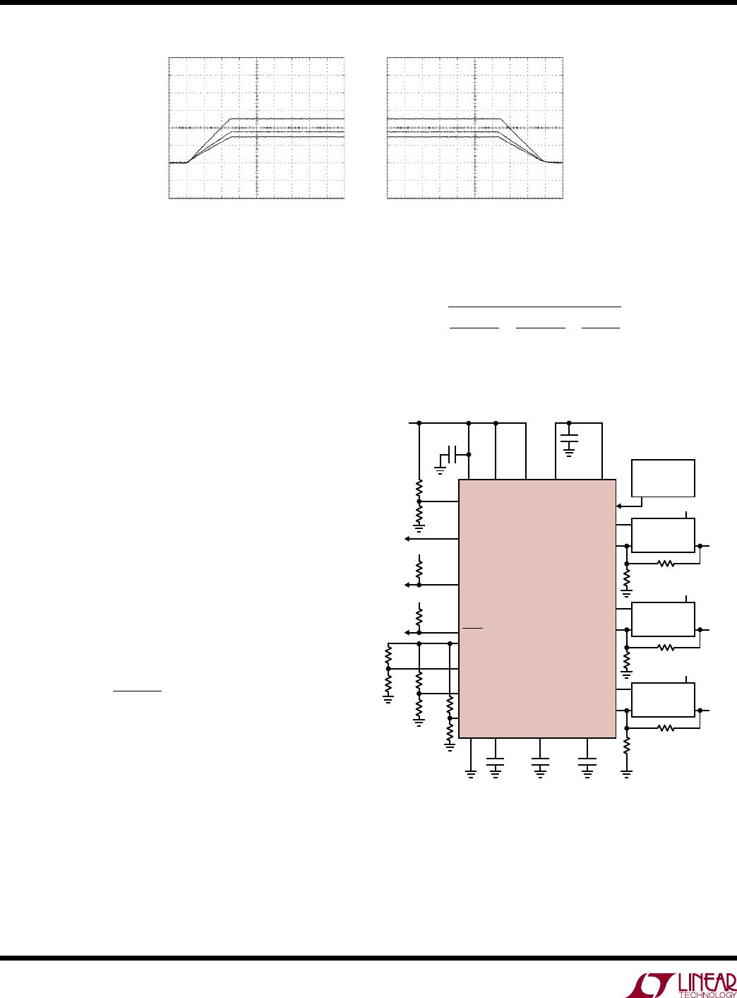
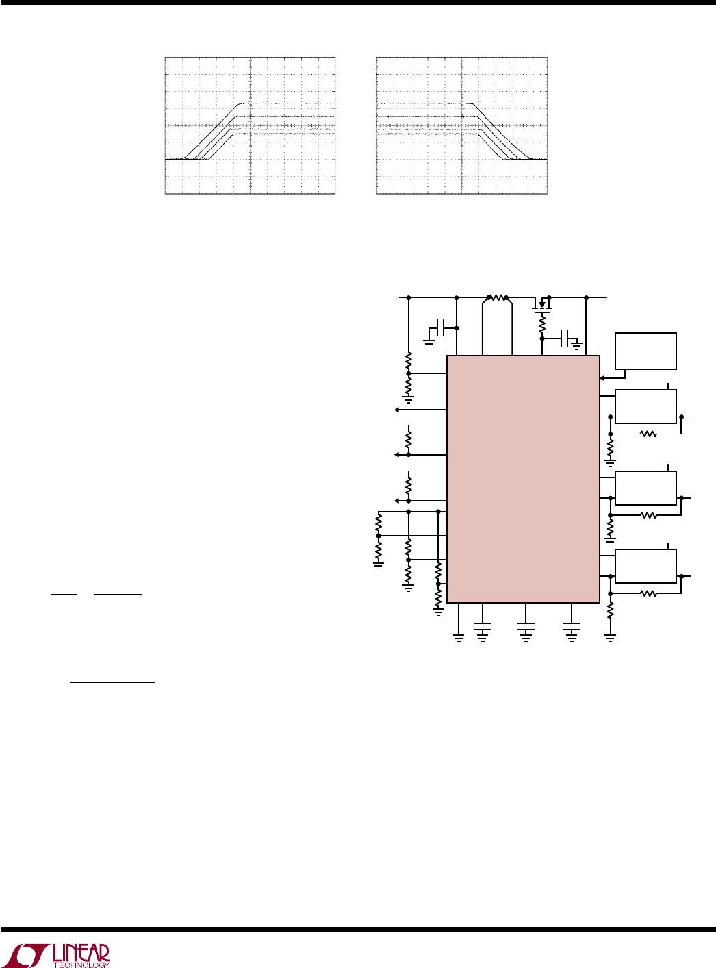
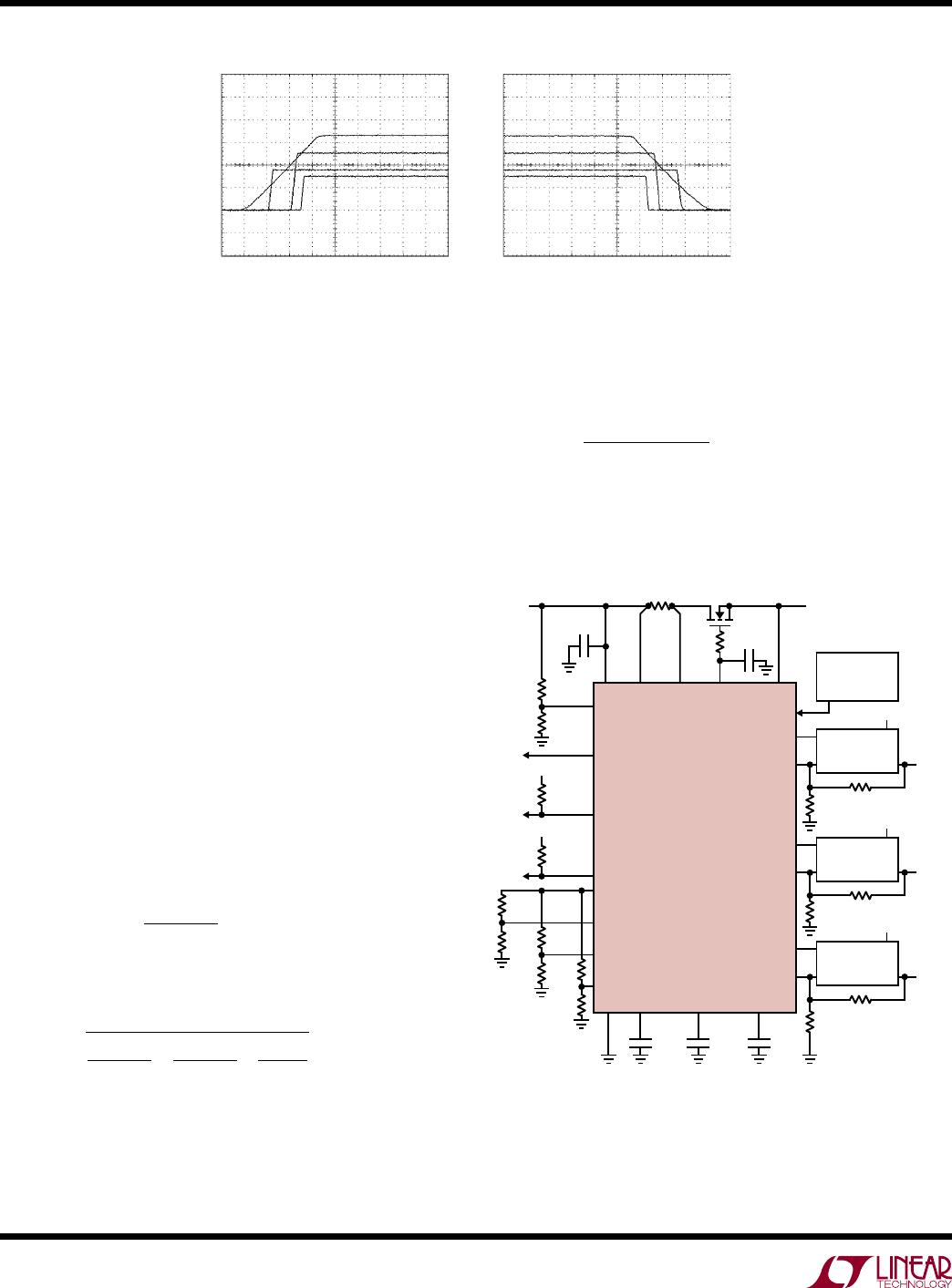
Supply Sequencing Example
In Figure 17, the three slave supplies are sequenced in-
stead of tracking. As in the coincident tracking example,
the 3.3V
master supply ramps up at
100V/s through an
external FET, so step 1 remains the same. The 1.8V slave
1 supply ramps up at 1000V/s beginning 10ms after the
master signal starts to ramp up. The 2.5V slave 2 supply
ramps up at 1000V/s beginning 20ms after the master
signal begins to ramp up. The 1.5V slave 3 supply ramps
up at 1000V/s beginning 25ms after the master signal
begins to ramp up. Note that not every combination of
ramp rates and delays is possible. Small delays and large
ratios of slave ramp rate to master ramp rate may result
in solutions that require negative resistors. In such cases,
either the delay must be increased or the ratio of slave
ramp rate to master ramp rate must be reduced. In this
example, solving for the slave 1 supply yields:
2. Solve for the pair of resistors that provide the desired
slave supply behavior, assuming no delay.
From Equation 2:
Rk
Vs
Vs
k
TB
=• ≈16 5
100
1000
165.
/
/
.
From Equation 3:
R
V
V
V
k
TA
ʹ=
+
≈
1 235
1 235
08
213
.
.
–
.
–.
SLAVE2
MASTER
SLAVE1
1V/DIV
1V/DIV
SLAVE3
10ms/DIV 10ms/DIV
2925 F17
Figure 17. Supply Sequencing from Figure 18
3. Choose R
TA
to obtain the desired delay.
From Equation 4:
R
Vk
ms Vs
k
TA
08 165
10 100
132
.•.
•/
.
From Equation 5:
Rkkk
TA
=≈–. || ..213132 348
0.015Ω
Si4412ADY
0.1µF
C
PGTMR
0.82µF
10k
V
CC
SENSEP SENSEN
3.3V
V
IN
3.3V
R
ONB
138k
3.3V V
IN
R
TB1
1.65k
R
TB2
8.87k
R
FA2
41.2k
2.5V
SLAVE2
MASTER
R
FB2
88.7k
R
TA2
4.87k
R
TB3
8.66k
R
TA3
3.74k
R
TA1
3.48k
R
ONA
100k
RAMPBUF
TRACK1
TRACK2
TRACK3
FB2
GATE
LTC2925
PGTMR
C
SDTMR
0.082µF
SDTMR
C
SCTMR
0.41µF
SCTMR
GND
2925 F18
RAMP
R
FA3
100k
1.5V
SLAVE3
R
FB3
86.6k
DC/DC
IN
FB = 0.8V OUT
DC/DC
IN
FB = 0.8V
RUN/SS
RUN/SS
OUT
FB3
3.3V
PGI
R
FA1
35.7k
1.8V
SLAVE1
R
FB1
16.5k
SUPPLY
MONITOR
DC/DC
IN
FB = 1.235V
RUN/SS
OUT
FB1
FAULT
ON
10k
V
IN
STATUS
REMOTE
RST
SD3
SD2
SD1
C
GATE
0.1µF
10Ω
Figure 18. Supply Sequencing Example