LTC2925
19
2925fd
For more information www.linear.com/LTC2925
applicaTions inForMaTion
Final Sanity Checks
The collection of equations below is useful for identifying
unrealizable solutions.
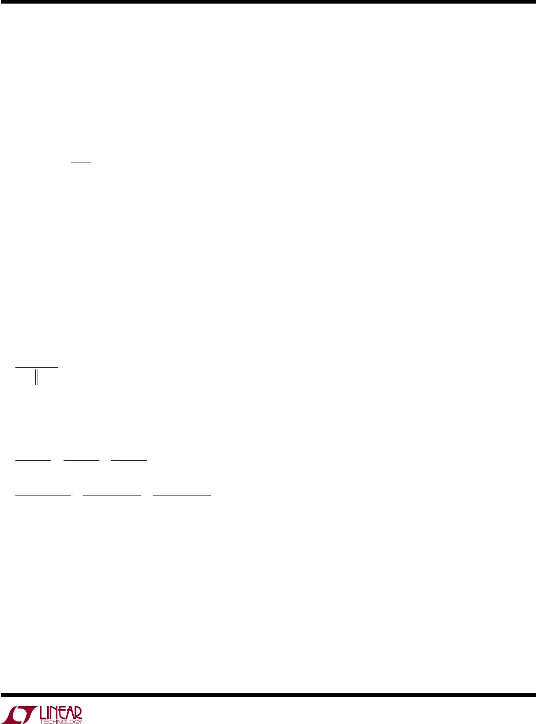
As stated in step 2, the slave supply must finish ramping
before the master signal has reached its final voltage. This
can be verified by the following equation:
V
R
R
V
TRACK
TB
TA
MASTER
1+
<
Here, V
TRACK
= 0.8V. V
MASTER
is the final voltage of the
master signal, either the supply voltage ramped up through
the optional external FET or V
CC
when no FET is present.
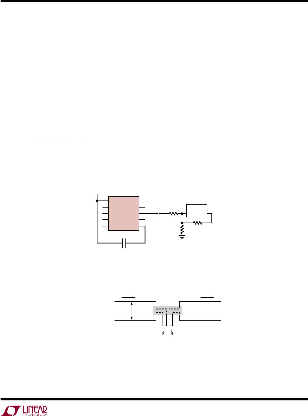
It is possible to choose resistor values that require the
LTC2925 to supply more current than the Electrical Char
-
acteristics table guarantees. To avoid this condition, check
that I
TRACKx
does not exceed 1mA and I
RAMPBUF
does not
exceed ±3mA.
To confirm that I
TRACKx
< 1mA, the TRACKx pin(s) maxi-
mum guaranteed current, verify that:
V
RR
mA
TRACK
TA TB
< 1
Finally, check that the RAMPBUF pin will not be forced to
sink more than 3mA when it is at 0V or be forced to source
more than 3mA when it is at V
MASTER
.
V
R
V
R
V
R
3mA and
V
RR
V
RR
V
RR
3mA
TRACK
TB1
TRACK
TB2
TRACK
TB3
MASTER
TA1 TB1
MASTER
TA2 TB2
MASTER
TA3 TB3
++<
+
+
+
+
+
<
Caution with Boost Regulators and Linear Regulators
Note that the LTC2925’s tracking cell is not able to control
the outputs of all types of power supplies. If it is necessary
to control a supply, where the output is not controllable
through its feedback node, the series FET can be used to
control its output. For example, boost regulators commonly
contain an inductor and diode between the input supply
and the output supply providing a DC current path when
the output voltage falls below the input voltage. Therefore,
the LTC2925’s tracking cell will not effectively drive the
supply’s output below the input.
Special caution should be taken when considering the use
of linear regulators. Three-terminal linear regulators have
a reference voltage that is referred to the output supply
rather than to ground. In this case, driving current into
the regulators feedback node will cause its output to rise
rather than fall. Even linear regulators that have their ref
-
erence voltage referred to ground, including low-dropout
regulators (LDOs), may be problematic. Linear regulators
commonly contain cir
cuitr
y that prevents driving their
outputs below their reference voltage. This may not be
obvious from the data sheets, so lab testing is recom
-
mended whenever the LTC2925’s tracking cell is used to
control linear regulators.
LTC2925
20
2925fd
For more information www.linear.com/LTC2925
applicaTions inForMaTion
Load Requirements
When the supplies are ramped down quickly, either the
load or the supply itself must be capable of sinking enough
current to support the ramp rate. For example, if there
is a large output capacitance on the supply and a weak
resistive load, supplies that do not sink current will have
their falling ramp rate limited by the RC time constant of
the load and the output capacitance. Figure 19 shows the
case when the 2.5V supply does not track the 1.8V and
3.3V supplies near ground.
Start-Up Delays
Often power supplies do not start-up immediately when
their input supplies are applied. If the LTC2925 tries to
ramp-up these power supplies as soon as the input sup
-
ply is present, the start-up of the outputs may be delayed
defeating the tracking cir
cuit (Figure 20). Often this delay
is intentionally configured by a soft-start capacitor
. This
can be remedied either by reducing the soft-start capacitor
on the slave supply or by increasing the shutdown timer
cycle configured by C
SDTMR
.
1V/DIV
MASTER
SLAVE2
SLAVE1
1ms/DIV
2925 F19
1V/DIV
MASTER
SLAVE1
SLAVE2
1ms/DIV
2925 F20
ON
Figure 19. Weak Resistive Load
Figure 20. Power Supply Start-Ups Delayed
LTC2925
21
2925fd
For more information www.linear.com/LTC2925
applicaTions inForMaTion
Layout Considerations
Be sure to place a 0.1µF bypass capacitor as near as pos-
sible to the supply pin of the LTC2925.
T
o minimize the noise on the slave supplies
outputs, keep
the traces connecting the FBx pins of the LTC2925 and the
feedback nodes of the slave supplies as short as possible.
In addition, do not route those traces next to signals with
fast transition times. In some circumstances it might be
advantageous to add a resistor near the feedback node of
the slave supply in series with the FBx pin of the LTC2925.
This resistor must not exceed:
R
VV
I
V
V
RR
SERIES
FB
MAXFB
FA F
==
16
16
1
.–
.
–|
|
BB
()
This resistor is most effective if there is already a
capacitor at the feedback node of the slave supply (often
a compensation component). Increasing the capacitance
on a slave supply
s feedback node will further improve the
noise immunity, but could affect the stability and transient
response of the supply.
For proper circuit breaker operation, Kelvin-sense PCB
connections between the sense resistor and the LTC2925’s
SENSEP and SENSEN pins are strongly recommended.
The drawing in Figure 22 illustrates the correct way of
making connections between the LTC2925 and the sense
resistor. PCB layout should be balanced and symmetrical to
minimize wiring errors. In addition, the PCB layout for the
sense resistor should include good thermal management
techniques for optimal sense resistor power dissipation.
The power rating of the sense resistor should accommodate
steady-state fault current levels so that the component is
not damaged before the circuit breaker trips.
R
FA
R
FB
R
SERIES
MINIMIZE
TRACE
LENGTH
V
CC
LTC2925
2925 F21
FB1
GND
0.1µF
DC/DC
FB OUT
IRC-TT SENSE RESISTOR
LR251201R010F
OR EQUIVALENT
0.01Ω, 1%, 1W
CURRENT FLOW
TO LOAD
TO
SENSEP
TO
SENSEN
CURRENT FLOW
TO LOAD
TRACK WIDTH W:
0.03" PER AMP
ON 1 OZ COPPER
2925 F22
W
Figure 21. Layout Considerations
Figure 22. Making PCB Connections to the Sense Resistor

LTC2925IUF#PBF

Mfr. #:
Manufacturer:
Analog Devices Inc.
Description:
Power Management Specialized - PMIC Pwr Supply Sequence/Tracking Controller
Lifecycle:
New from this manufacturer.
Delivery:
DHL FedEx Ups TNT EMS
Payment:
T/T Paypal Visa MoneyGram Western Union