Register and PLL Specifications
Table 12: Register Specifications
SSTU32866 devices or equivalent
Parameter Symbol Pins Condition Min Max Units
DC high-level
input voltage
V
IH(DC)
Control, command,
address
SSTL_18 V
REF(DC)
+ 125 V
DDQ
+ 250 mV
DC low-level
input voltage
V
IL(DC)
Control, command,
address
SSTL_18 0 V
REF(DC)
- 125 mV
AC high-level
input voltage
V
IH(AC)
Control, command,
address
SSTL_18 V
REF(DC)
+ 250 mV
AC low-level
input voltage
V
IL(AC)
Control, command,
address
SSTL_18 V
REF(DC)
- 250 mV
Output high
voltage
V
OH
Parity output LVCMOS 1.2 V
Output low voltage V
OL
Parity output LVCMOS 0.5 V
Input current I
I
All pins V
I
= V
DD
or V
SS
±0.5 µA
Static standby I
DD
All pins RESET# = V
SSQ
(I
O
= 0) 100 µA
Static operating I
DD
All pins RESET# = V
SS
; V
I
= V
IH(AC)
or V
IL(DC)
I
O
= 0
40 mA
Dynamic operating
(clock tree)
I
DDD
N/A RESET# = V
DD
;
V
I
= V
IH(DC)
or V
IL(AC)
,
I
O
= 0; CK and CK#
switching 50% duty cy-
cle
Varies by
manufacturer
µA
Dynamic operating
(per each input)
I
DDD
N/A RESET# = V
DD
;
V
I
= V
IH(AC)
or V
IL(DC)
,
I
O
= 0; CK and CK#
switching 50% duty
cycle; One data in/out
switching at
t
CK/2,
50% duty cycle
Varies by
manufacturer
µA
Input capacitance
(per device, per pin)
C
IN
All inputs except
RESET#
V
I
= V
REF
±250mV;
V
DD
= 1.8V
2.5 3.5 pF
Input capacitance
(per device, per pin)
C
IN
RESET# V
I
= V
DD
or V
SS
Varies by
manufacturer
Varies by
manufacturer
pF
Note:
1. Timing and switching specifications for the register listed are critical for proper opera-
tion of the DDR2 SDRAM RDIMMs. These are meant to be a subset of the parameters for
the specific device used on the module. Detailed information for this register is available
in JEDEC standard JESD82.
512MB, 1GB (x72, ECC, SR) 244-Pin DDR2 SDRAM Mini-RDIMM
Register and PLL Specifications
PDF: 09005aef83f993e9
htf9c64_128x72pkz.pdf – Rev. C 4/14 EN
13
Micron Technology, Inc. reserves the right to change products or specifications without notice.
© 2010 Micron Technology, Inc. All rights reserved.
Table 13: PLL Specifications
CU877 device or equivalent
Parameter Symbol Pins Condition Min Max Units
DC high-level
input voltage
V
IH
RESET# LVCMOS 0.65 × V
DD
V
DC low-level
input voltage
V
IL
RESET# LVCMOS 0.35 × V
DD
V
Input voltage (limits) V
IN
RESET#, CK,
CK#
- 0.3 V
DD
+ 0.3 V
DC high-level
input voltage
V
IH
CK, CK# Differential input 0.65 × V
DD
V
DC low-level
input voltage
V
IL
CK, CK# Differential input 0.35 × V
DD
V
Input differential-pair
cross voltage
V
IX
CK, CK# Differential input (V
DDQ
/2) - 0.15 (V
DD
/2) + 0.15 V
Input differential
voltage
V
ID(DC)
CK, CK# Differential input 0.3 V
DD
+ 0.4 V
Input differential
voltage
V
ID(AC)
CK, CK# Differential input 0.6 V
DD
+ 0.4 V
Input current I
I
RESET# V
I
= V
DD
or V
SS
–10 10 µA
CK, CK# V
I
= V
DD
or V
SS
–250 250 µA
Output disabled
current
I
ODL
RESET# = V
SS
; V
I
= V
IH(AC)
or V
IL(DC)
100 µA
Static supply current I
DDLD
CK = CK# = LOW 500 µA
Dynamic supply I
DD
N/A CK, CK# = 270 MHz, all
outputs open (not con-
nected to PCB)
300 mA
Input capacitance C
IN
Each input V
I
= V
DD
or V
SS
2 3 pF
Table 14: PLL Clock Driver Timing Requirements and Switching Characteristics
Parameter Symbol Min Max Units
Stabilization time
t
L 15 μs
Input clock slew rate slr(i) 1.0 4.0 V/ns
SSC modulation frequency 30 33 kHz
SSC clock input frequency deviation 0.0 –0.5 %
PLL loop bandwidth (–3dB from unity gain) 2.0 MHz
Note:
1. PLL timing and switching specifications are critical for proper operation of the DDR2
DIMM. This is a subset of parameters for the specific PLL used. Detailed PLL information
is available in JEDEC standard JESD82.
512MB, 1GB (x72, ECC, SR) 244-Pin DDR2 SDRAM Mini-RDIMM
Register and PLL Specifications
PDF: 09005aef83f993e9
htf9c64_128x72pkz.pdf – Rev. C 4/14 EN
14
Micron Technology, Inc. reserves the right to change products or specifications without notice.
© 2010 Micron Technology, Inc. All rights reserved.
Serial Presence-Detect
For the latest SPD data, refer to Micron's SPD page: www.micron.com/SPD.
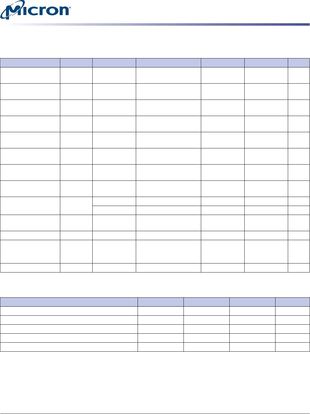
Table 15: SPD EEPROM Operating Conditions
Parameter/Condition Symbol Min Max Units
Supply voltage V
DDSPD
1.7 3.6 V
Input high voltage: logic 1; All inputs V
IH
V
DDSPD
× 0.7 V
DDSPD
+ 0.5 V
Input low voltage: logic 0; All inputs V
IL
–0.6 V
DDSPD
× 0.3 V
Output low voltage: I
OUT
= 3mA V
OL
0.4 V
Input leakage current: V
IN
= GND to V
DD
I
LI
0.1 3 µA
Output leakage current: V
OUT
= GND to V
DD
I
LO
0.05 3 µA
Standby current I
SB
1.6 4 µA
Power supply current, READ: SCL clock frequency = 100 kHz I
CCR
0.4 1 mA
Power supply current, WRITE: SCL clock frequency = 100 kHz I
CCW
2 3 mA
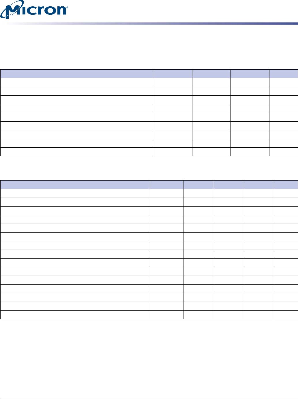
Table 16: SPD EEPROM AC Operating Conditions
Parameter/Condition Symbol Min Max Units Notes
SCL LOW to SDA data-out valid
t
AA 0.2 0.9 µs 1
Time bus must be free before a new transition can start
t
BUF 1.3 µs
Data-out hold time
t
DH 200 ns
SDA and SCL fall time
t
F 300 ns 2
SDA and SCL rise time
t
R 300 ns 2
Data-in hold time
t
HD:DAT 0 µs
Start condition hold time
t
HD:STA 0.6 µs
Clock HIGH period
t
HIGH 0.6 µs
Noise suppression time constant at SCL, SDA inputs
t
I 50 ns
Clock LOW period
t
LOW 1.3 µs
SCL clock frequency
t
SCL 400 kHz
Data-in setup time
t
SU:DAT 100 ns
Start condition setup time
t
SU:STA 0.6 µs 3
Stop condition setup time
t
SU:STO 0.6 µs
WRITE cycle time
t
WRC 10 ms 4
Notes:
1. To avoid spurious start and stop conditions, a minimum delay is placed between SCL = 1
and the falling or rising edge of SDA.
2. This parameter is sampled.
3. For a restart condition or following a WRITE cycle.
4. The SPD EEPROM WRITE cycle time (
t
WRC) is the time from a valid stop condition of a
write sequence to the end of the EEPROM internal ERASE/PROGRAM cycle. During the
WRITE cycle, the EEPROM bus interface circuit is disabled, SDA remains HIGH due to
pull-up resistance, and the EEPROM does not respond to its slave address.
512MB, 1GB (x72, ECC, SR) 244-Pin DDR2 SDRAM Mini-RDIMM
Serial Presence-Detect
PDF: 09005aef83f993e9
htf9c64_128x72pkz.pdf – Rev. C 4/14 EN
15
Micron Technology, Inc. reserves the right to change products or specifications without notice.
© 2010 Micron Technology, Inc. All rights reserved.

MT9HTF12872PKZ-80EH1

Mfr. #:
Manufacturer:
Micron
Description:
DRAM Module DDR2 SDRAM 1Gbyte 244MiniRDIMM
Lifecycle:
New from this manufacturer.
Delivery:
DHL FedEx Ups TNT EMS
Payment:
T/T Paypal Visa MoneyGram Western Union