Isolated Precision Half-Bridge Driver,
4 A Output
Data Sheet
ADuM3223/ADuM4223
Rev. I Document Feedback
Information furnished by Analog Devices is believed to be accurate and reliable. However, no
responsibility is assumed by Analog Devices for its use, nor for any infringements of patents or other
rights of third parties that may result from its use. Specifications subject to change without notice. No
license is granted by implication or otherwise under any patent or patent rights of Analog Devices.
Trademarks and registered trademarks are the property of their respective owners.
One Technology Way, P.O. Box 9106, Norwood, MA 02062-9106, U.S.A.
Tel: 781.329.4700 ©2012–2017 Analog Devices, Inc. All rights reserved.
Technical Support www.analog.com
FEATURES
4 A peak output current
Working voltage
High-side or low-side relative to input: 537 V peak
High-side to low-side differential: 800 V peak
High frequency operation: 1 MHz maximum
3.3 V to 5 V CMOS input logic
4.5 V to 18 V output drive
UVLO at 2.5 V V
DD1
ADuM3223A/ADuM4223A UVLO at 4.1 V V
DD2
ADuM3223B/ADuM4223B UVLO at 7.0 V V
DD2
ADuM3223C/ADuM4223C UVLO at 11.0 V V
DD2
Precise timing characteristics
54 ns maximum isolator and driver propagation delay
5 ns maximum channel-to-channel matching
CMOS input logic levels
High common-mode transient immunity: >25 kV/μs
Enhanced system-level ESD performance per IEC 61000-4-x
High junction temperature operation: 125°C
Thermal shutdown protection
Default low output
Safety and regulatory approvals
ADuM3223 narrow-body, 16-lead SOIC
UL recognition per UL 1577
3000 V rms for 1 minute SOIC long package
CSA Component Acceptance Notice 5A
VDE certificate of conformity
DIN V VDE V 0884-10 (VDE V 0884-10):2006-12
V
IORM
= 560 V peak
ADuM4223 wide-body, 16-lead SOIC
UL recognition per UL 1577
5000 V rms for 1 minute SOIC long package
CSA Component Acceptance Notice 5A
VDE certificate of conformity
DIN V VDE V 0884-10 (VDE V 0884-10):2006-12
V
IORM
= 849 V peak
Qualified for automotive applications
APPLICATIONS
Switching power supplies
Isolated IGBT/MOSFET gate drives
Industrial inverters
Automotive
FUNCTIONAL BLOCK DIAGRAM
Figure 1.
GENERAL DESCRIPTION
The ADuM3223/ADuM4223
1
are 4 A isolated, half-bridge gate
drivers that employ the Analog Devices, Inc., iCoupler® technology
to provide independent and isolated high-side and low-side
outputs. The ADuM3223 provides 3000 V rms isolation in the
narrow body, 16-lead SOIC package, and the ADuM4223 provides
5000 V rms isolation in the wide body, 16-lead SOIC package.
Combining high speed CMOS and monolithic transformer
technology, these isolation components provide outstanding
performance characteristics superior to the alternatives, such as
the combination of pulse transformers and gate drivers.
The ADuM3223/ADuM4223 isolators each provide two
independent isolated channels. They operate with an input
supply ranging from 3.0 V to 5.5 V, providing compatibility with
lower voltage systems. In comparison to gate drivers employing
high voltage level translation methodologies, the ADuM3223/
ADuM4223 offer the benefit of true, galvanic isolation between
the input and each output. Each output may be continuously
operated up to 537 V peak relative to the input, thereby supporting
low-side switching to negative voltages. The differential voltage
between the high-side and low-side may be as high as 800 V peak.
As a result, the ADuM3223/ADuM4223 provide reliable control
over the switching characteristics of IGBT/MOSFET configurations
over a wide range of positive or negative switching voltages.
1
Protected by U.S. Patents 5,952,849; 6,873,065; 7,075,239. Other patents pending.
ENCODE DECODE
ENCODE DECODE
DISABLE
NC
NC
V
DD1
NC
V
DDB
V
OB
GND
B
5
6
7
8
12
11
GND
1
NC
4 13
V
DD1
GND
A
3 14
V
IB
V
OA
2 15
V
IA
V
DDA
1 16
10
9
NC = NO CONNECT
ADuM3223/
ADuM4223
10450-001
ADuM3223/ADuM4223 Data Sheet
Rev. I | Page 2 of 20
TABLE OF CONTENTS
Features .............................................................................................. 1
Applications ....................................................................................... 1
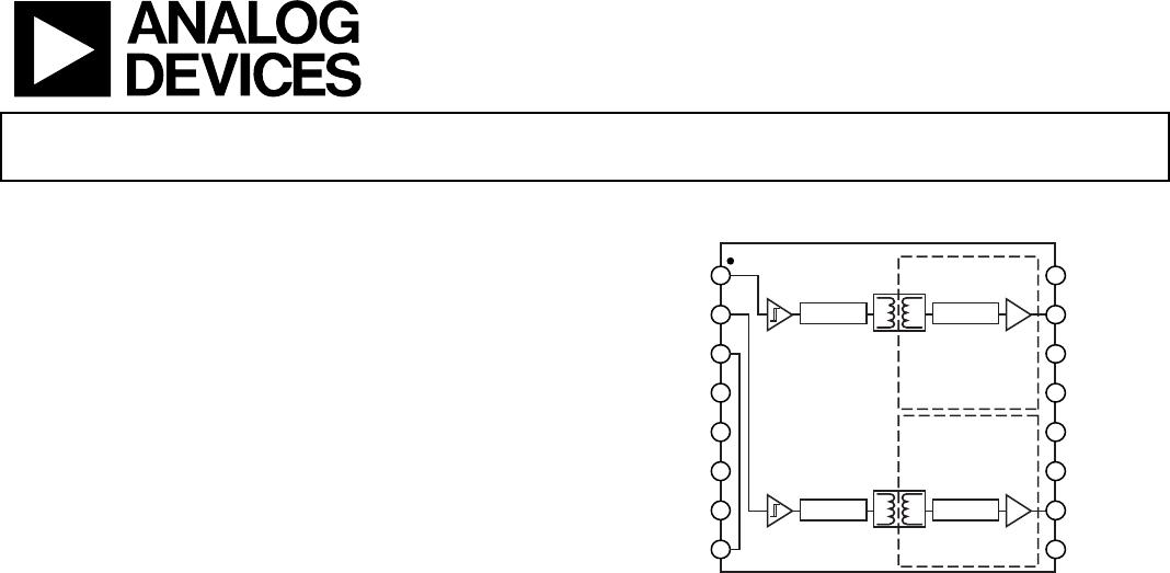
Functional Block Diagram .............................................................. 1
General Description ......................................................................... 1
Revision History ............................................................................... 2
Specifications ..................................................................................... 3
Electrical Characteristics—5 V Operation ................................ 3
Electrical Characteristics—3.3 V Operation ............................. 4
Package Characteristics ............................................................... 5
Insulation and Safety-Related Specifications ............................ 5
Regulatory Information ............................................................... 6
DIN V VDE V 0884-10 (VDE V 0884-10) Insulation
Characteristics .............................................................................. 7
Recommended Operating Conditions ...................................... 8
Absolute Maximum Ratings ............................................................ 9
ESD Caution...................................................................................9
Pin Configuration and Function Descriptions ........................... 11
Typical Performance Characteristics ........................................... 12
Applications Information .............................................................. 15
PC Board Layout ........................................................................ 15
Propagation Delay-Related Parameters ................................... 15
Thermal Limitations and Switch Load Characteristics ......... 15
Output Load Characteristics ..................................................... 15
Boot-Strapped Half-Bridge Operation .................................... 16
DC Correctness and Magnetic Field Immunity .......................... 16
Power Consumption .................................................................. 17
Insulation Lifetime ..................................................................... 18
Outline Dimensions ....................................................................... 19
Ordering Guide .......................................................................... 20
Automotive Products ................................................................. 20
REVISION HISTORY
3/2017—Rev. H to Rev. I
Changes to Table 14 ........................................................................ 11
1/2017—Rev. G to Rev. H
Changes to Table 13 ........................................................................ 10
11/2015—Rev. F to Rev. G
Changes to Power Consumption Section .................................... 17
7/2015—Rev. E to Rev. F
Changes to Features Section............................................................ 1
Changes to Table 6 and Table 7 ....................................................... 6
Changes to Power Consumption Section .................................... 17
11/2014—Rev. D to Rev. E
Changes to Features Section and General Description
Section ................................................................................................ 1
Changes to Table 5 ............................................................................ 5
Changes to Regulatory Information Section, Table 6, and
Table 7 ................................................................................................ 6
Changes to Table 8 and Table 9 ....................................................... 7
4/2014—Rev. C to Rev. D
Changes to Applications Section .................................................... 1
Changes to Insulation Lifetime Section ....................................... 18
Changes to Ordering Guide .......................................................... 20
12/2013—Rev. B to Rev. C
Change to Features Section ............................................................. 1
Changes to Switching Specifications Parameter, Table 1 ............. 3
Added Thermal Shutdown Temperatures Parameter, Table 1 ..... 3
Changes to Switching Specifications Parameter, Table 2 ............. 4
Added Thermal Shutdown Temperatures Parameter, Table 2 ..... 4
Changes to Table 10 .......................................................................... 8
Change to Figure 13 Caption ........................................................ 13
Changes to Thermal Limitations and Switch Load
Characteristics Section .................................................................. 15
Change to Boot-Strapped Half-Bridge Operation Section ....... 16
5/2013—Rev. A to Rev. B
Added V
DDA
, V
DDB
Rise Time of 0.5 V/µs; Table 10 ....................... 8
Changes to Figure 22...................................................................... 16
1/2013—Rev. 0 to Rev. A
Added Automotive Information (Throughout) ............................ 1
Updated Safety and Regulatory Approvals (Throughout) ........... 1
Changed High-Side to Low-Side Differential from 700 V
DC PEAK
to 800 V peak ..................................................................................... 1
Added R
OA
, R
OB
Minimum and Maximum Values, Table 1 ......... 3
Added R
OA
, R
OB
Minimum and Maximum Values, Table 2 ......... 4
Changes to Table 13 ....................................................................... 10
Changes to Figure 19...................................................................... 15
Added Boot-Strapped Half Bridge Operation Section and
Figure 22; Renumbered Sequentially ........................................... 16
Changes to Ordering Guide .......................................................... 20
5/2012—Revision 0: Initial Version
Data Sheet ADuM3223/ADuM4223
Rev. I | Page 3 of 20
SPECIFICATIONS
ELECTRICAL CHARACTERISTICS—5 V OPERATION
All voltages are relative to their respective ground. 4.5 V ≤ V
DD1
≤ 5.5 V, 4.5 V ≤ V
DD2
≤ 18 V, unless stated otherwise. All minimum/
maximum specifications apply over T
J
= −40°C to 125°C. All typical specifications are at T
J
= 25°C, V
DD1
= 5 V, V
DD2
= 12 V. Switching
specifications are tested with CMOS signal levels.
Table 1.
Parameter Symbol Min Typ Max Unit Test Conditions
DC SPECIFICATIONS
Input Supply Current, Quiescent I
DDI(Q)
1.4 2.4 mA
Output Supply Current, Per Channel, Quiescent I
DDO(Q)
2.3 3.2 mA
Supply Current at 1 MHz
V
DD1
Supply Current I
DD1(Q)
1.6 2.5 mA Up to 1 MHz, no load
V
DDA
/V
DDB
Supply Current I
DDA
/I
DDB(Q)
5.6 8.0 mA Up to 1 MHz, no load
Input Currents I
IA
, I
IB
−1 +0.01 +1 μA 0 V
IA
, V
IB
≤ V
DD1
Logic High Input Threshold V
IH
0.7 × V
DD1
V
Logic Low Input Threshold V
IL
0.3 × V
DD1
V
Logic High Output Voltages V
OAH
, V
OBH
V
DD2
– 0.1 V
DD2
V I
Ox
= −20 mA, V
Ix
= V
IxH
Logic Low Output Voltages V
OAL
, V
OBL
0.0 0.15 V I
Ox
= +20 mA, V
Ix
= V
IxL
Undervoltage Lockout, V
DD2
Supply
Positive Going Threshold V
DD2UV+
4.1 4.4 V A-grade
Negative Going Threshold V
DD2UV−
3.2 3.6 V A-grade
Hysteresis V
DD2UVH
0.5 V A-grade
Positive Going Threshold V
DD2UV+
6.9 7.4 V B-grade
Negative Going Threshold V
DD2UV−
5.7 6.2 V B-grade
Hysteresis V
DD2UVH
0.7 V B-grade
Positive Going Threshold V
DD2UV+
10.5 11.1 V C-grade
Negative Going Threshold V
DD2UV−
8.9 9.6 V C-grade
Hysteresis V
DD2UVH
0.9 V C-grade
Output Short-Circuit Pulsed Current
1
I
OA(SC)
, I
OB(SC)
2.0 4.0 A V
DD2
= 12 V
Output Pulsed Source Resistance R
OA
, R
OB
0.3 1.1 3.0 Ω V
DD2
= 12 V
Output Pulsed Sink Resistance R
OA
, R
OB
0.3 0.6 3.0 Ω V
DD2
= 12 V
THERMAL SHUTDOWN TEMPERATURES
Junction Temperature Shutdown, Rising Edge T
JR
150 °C
Junction Temperature Shutdown, Falling Edge T
JF
140 °C
SWITCHING SPECIFICATIONS
Pulse Width
2
PW 50 ns C
L
= 2 nF, V
DD2
= 12 V
Maximum Data Rate
3
1 MHz C
L
= 2 nF, V
DD2
= 12 V
Propagation Delay
4
t
DHL
, t
DLH
31 43 54 ns C
L
= 2 nF, V
DD2
= 12 V; see Figure 20
ADuM3223A/ADuM4223A t
DHL
, t
DLH
35 47 59 ns C
L
= 2 nF, V
DD2
= 4.5 V; see Figure 20
Propagation Delay Skew
5
t
PSK
12 ns C
L
= 2 nF, V
DD2
= 12 V; see Figure 20
Channel-to-Channel Matching
6
t
PSKCD
1 5 ns C
L
= 2 nF, V
DD2
= 12 V; see Figure 20
t
PSKCD
1 7 ns C
L
= 2 nF, V
DD2
= 4.5 V; see Figure 20
Output Rise/Fall Time (10% to 90%) t
R
/t
F
6 12 18 ns C
L
= 2 nF, V
DD2
= 12 V; see Figure 20
Dynamic Input Supply Current Per Channel I
DDI(D)
0.05 mA/Mbps V
DD2
= 12 V
Dynamic Output Supply Current Per Channel I
DDO(D)
1.65 mA/Mbps V
DD2
= 12 V
Refresh Rate f
r
1.2 Mbps
1
Short-circuit duration less than 1 μs. Average power must conform to the limit shown under the Absolute Maximum Ratings.
2
The minimum pulse width is the shortest pulse width at which the specified timing parameter is guaranteed.
3
The maximum data rate is the fastest data rate at which the specified timing parameter is guaranteed.
4
t
DLH
propagation delay is measured from the time of the input rising logic high threshold, V
IH
, to the output rising 10% level of the V
Ox
signal. t
DHL
propagation delay is
measured from the input falling logic low threshold, V
IL
, to the output falling 90% threshold of the V
Ox
signal. See Figure 20 for waveforms of propagation delay
parameters.
5
t
PSK
is the magnitude of the worst-case difference in t
DLH
and/or t
DHL
that is measured between units at the same operating temperature, supply voltages, and output
load within the recommended operating conditions. See Figure 20 for waveforms of propagation delay parameters.
6
Channel-to-channel matching is the absolute value of the difference in propagation delays between the two channels.

ADUM3223ARZ

Mfr. #:
Manufacturer:
Analog Devices Inc.
Description:
Gate Drivers 3kV RMS Prec Half- Bridge Dvr 4A Out
Lifecycle:
New from this manufacturer.
Delivery:
DHL FedEx Ups TNT EMS
Payment:
T/T Paypal Visa MoneyGram Western Union