ADuM3223/ADuM4223 Data Sheet
Rev. I | Page 16 of 20
The following equation defines the Q factor of the RLC circuit,
which indicates how the ADuM3223/ADuM4223 output responds
to a step change. For a well-damped output, Q is less than 1.
Adding a series gate resistance dampens the output response.
GS
TRACE
GATE
SW
C
L
RR
Q
)(
1
In Figure 5, the ADuM3223/ADuM4223 output waveforms for
a 12 V output are shown for a C
GS
of 2 nF. Note the small amount of
ringing of the output in Figure 5 with C
GS
of 2 nF, R
SW
of 1.1 Ω,
R
GATE
of 0 Ω, and a calculated Q factor of 0.75, where less than 1
is desired for good damping.
Output ringing can be reduced by adding a series gate resistance
to dampen the response. For applications of less than 1 nF load,
it is recommended to add a series gate resistor of about 2 Ω to 5 Ω.
BOOT-STRAPPED HALF-BRIDGE OPERATION
The ADuM3223/ADuM4223 are well suited to the operation of
two output gate signals that are referenced to separate grounds,
as in the case of a half-bridge configuration. Because isolated
auxiliary supplies are often expensive, it is beneficial to reduce
the amount of supplies. One method to perform this is to use a
boot-strap configuration for the high-side supply of the
ADuM3223/ADuM4223. In this topology, the decoupling
capacitor, C
A
, acts as the energy storage for the high-side supply,
and is filled whenever the low-side switch is closed, bringing
GND
A
to GND
B
. During the charging time of C
A
, the dv/dt of
the V
DDA
voltage must be controlled to reduce the possibility of
glitches on the output. Keeping the dv/dt below 10 V/µs is
recommended for the ADuM3223/ADuM4223. This can be
controlled by introducing a series resistance, R
BOOT
, into the
charging path of C
A
. As an example, if V
AUX
is 12 V, C
A
has a
total capacitance of 10 µF, and the forward voltage drop of the
bootstrap diode is 1 V:
11.0
V/10F10
V112
max
s
V
dt
dv
C
VV
R
A
BOOT
D
AUX
BOOT
DC CORRECTNESS AND MAGNETIC FIELD IMMUNITY
Positive and negative logic transitions at the isolator input cause
narrow (~1 ns) pulses to be sent to the decoder via the transformer.
The decoder is bistable and is, therefore, either set or reset by
the pulses, indicating input logic transitions. In the absence of
logic transitions of more than 1 µs at the input, a periodic set of
refresh pulses indicative of the correct input state are sent to
ensure dc correctness at the output.
If the decoder receives no internal pulses for more than about
3 µs, the input side is assumed to be unpowered or nonfunctional,
in which case, the isolator output is forced to a default low state
by the watchdog timer circuit. In addition, the outputs are in a
low default state while the power is coming up before the
UVLO threshold is crossed.
The ADuM3223/ADuM4223 is immune to external magnetic
fields. The limitation on the ADuM3223/ADuM4223 magnetic
field immunity is set by the condition in which induced voltage
in the transformer receiving coil is sufficiently large to either
falsely set or reset the decoder. The following analysis defines
the conditions under which this can occur. The 3 V operating
condition of the ADuM3223/ADuM4223 is examined because
it represents the most susceptible mode of operation. The pulses
at the transformer output have an amplitude greater than 1.0 V.
The decoder has a sensing threshold at about 0.5 V, therefore
establishing a 0.5 V margin in which induced voltages can be
tolerated. The voltage induced across the receiving coil is given by
V = (−dβ/dt) ∑π r
n
2
, n = 1, 2, ... , N
where:
β is the magnetic flux density (gauss).
N is the number of turns in the receiving coil.
r
n
is the radius of the nth turn in the receiving coil (cm).
Figure 22. Circuit of Bootstrapped Half-Bridge Operation
ENCODE DECODE
ENCODE DECODE
DISABLE
NC
NC
V
DD1
NC
V
DDB
V
OB
GND
B
5
6
7
8
12
11
GND
1
NC
4 13
V
DD1
GND
A
3 14
V
IB
V
OA
2 15
V
IA
V
DDA
1 16
10
9
NC = NO CONNECT
ADuM3223/
ADuM4223
C
A
C
B
V
AUX
R
BOOT
R
EXT_A
R
EXT_B
C
DD1
V
PRIM
V
PRIM
V
PRIM
2
1
V
BUS
V
D
BOOT
D
BOOT
10450-222
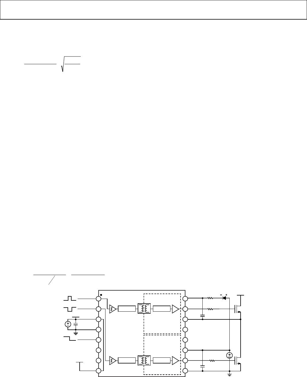
Data Sheet ADuM3223/ADuM4223
Rev. I | Page 17 of 20
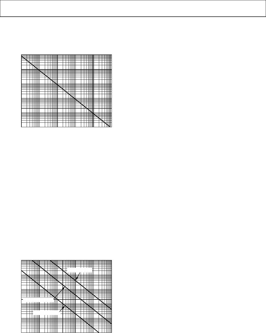
Given the geometry of the receiving coil in the ADuM3223/
ADuM4223 and an imposed requirement that the induced
voltage is, at most, 50% of the 0.5 V margin at the decoder, a
maximum allowable magnetic field is calculated, as shown in
Figure 23.
Figure 23. Maximum Allowable External Magnetic Flux Density
For example, at a magnetic field frequency of 1 MHz, the
maximum allowable magnetic field of 0.08 kgauss induces a
voltage of 0.25 V at the receiving coil. This is about 50% of the
sensing threshold and does not cause a faulty output transition.
Similarly, if such an event were to occur during a transmitted
pulse (and had the worst-case polarity), the received pulse is
reduced from >1.0 V to 0.75 V, still well above the 0.5 V sensing
threshold of the decoder.
The preceding magnetic flux density values correspond to
specific current magnitudes at given distances away from the
ADuM3223/ADuM4223 transformers. Figure 24 expresses
these allowable current magnitudes as a function of frequency
for selected distances. As shown, the ADuM3223/ADuM4223
are immune and only can be affected by extremely large currents
operated at a high frequency and very close to the component.
For the 1 MHz example, a 0.2 kA current must be placed 5 mm
away from the ADuM3223/ADuM4223 to affect the
components operation.
Figure 24. Maximum Allowable Current for Various
Current-to-ADuM3223/ADuM4223 Spacings
POWER CONSUMPTION
The supply current at a given channel of the ADuM3223/
ADuM4223 isolator is a function of the supply voltage,
channel data rate, and channel output load.
During the driving of a MOSFET gate, the driver must dissipate
power. This power is not insignificant and can lead to thermal
shutdown (TSD) if considerations are not made. The gate of a
MOSFET can be simulated approximately as a capacitive load.
Due to Miller capacitance and other nonlinearities, it is common
practice to take the stated input capacitance, C
ISS
, of a given
MOSFET and multiply it by a factor of 5 to arrive at a conservative
estimate to approximate the load being driven. With this value,
the estimated total power dissipation per channel due to
switching action is given by
P
DISS
= C
EST
× (V
DDx
)
2
× f
S
where:
C
EST
= C
ISS
× 5.
f
S
is the switching frequency.
Alternately, use the gate charge to obtain a more precise value
for P
DISS
.
P
DISS
= Q
GATE
× V
DDx
× f
S
where:
Q
GATE
is the gate charge for the MOSFET.
f
S
is the switching frequency.
This power dissipation is shared between the internal on
resistances of the internal gate driver switches and the external
gate resistances, R
GON
and R
GOFF
. The ratio of the internal gate
resistances to the total series resistance allows the calculation of
losses seen within the ADuM3223/ADuM4223 chips per
channel.
P
DISS_IC
= P
DISS
× ½ × (R
DSON_P
/(R
EXT_X
+ R
DSON_P
) +
R
DSON_N
/(R
EXT_X
+ R
DSON_N
))
Taking the power dissipation found inside the chip and
multiplying it by θ
JA
gives the rise above ambient temperature
that the ADuM3223/ADuM4223 experiences, multiplied by two
to reflect that there are two channels.
T
J
= θ
JA
× 2 × P
DISS_IC
+ T
AMB
For the device to remain within specification, T
J
must not
exceed 125°C. If T
J
exceeds 150°C (typical), the device enters TSD.
Quiescent power dissipation may also be added to give a more
accurate number for temperature rise, but the switching power
losses are often the largest source of power dissipation, and
quiescent losses can often be ignored. To calculate the total
supply current, the quiescent supply currents for each input and
output channel corresponding to I
DD1(Q)
, I
DDA(Q)
, and I
DDB(Q)
are
added. The full equation for the T
J
becomes
T
J
= θ
JA
× (2 × P
DISS_IC
+ V
DD1
× I
DD1(Q)
+ V
DDA
× I
DDA(Q)
+
V
DDB
× I
DDB(Q)
) + T
AMB
100
10
1
0.1
0.01
0.001
1k 10k 100k 1M 10M 100M
MAXIMUM ALLOWABLE MAGNETIC FLUX
DENSITY (kgauss)
MAGNETIC FIELD FREQUENCY (Hz)
10450-122
1k
100
10
1
0.1
0.01
1k 10k 100k 1M 10M 100M
MAXIMUM ALLOWABLE CURRENT (kA)
MAGNETIC FIELD FREQUENCY (Hz)
10450-123
DISTANCE = 1m
DISTANCE = 100mm
DISTANCE = 5mm
ADuM3223/ADuM4223 Data Sheet
Rev. I | Page 18 of 20
Figure 9 provides total input I
DD1
supply current as a function of
data rate for both input channels. Figure 10 provides total I
DDA
or I
DDB
supply current as a function of data rate for both outputs
loaded with 2 nF capacitance.
INSULATION LIFETIME
All insulation structures eventually break down when subjected to
voltage stress over a sufficiently long period. The rate of insulation
degradation is dependent on the characteristics of the voltage
waveform applied across the insulation. In addition to the
testing performed by the regulatory agencies, Analog Devices
carries out an extensive set of evaluations to determine the
lifetime of the insulation structure within the ADuM3223/
ADuM4223.
Analog Devices performs accelerated life testing using voltage
levels higher than the rated continuous working voltage.
Acceleration factors for several operating conditions are
determined. These factors allow calculation of the time to failure
at the actual working voltage.
The values shown in Table 12 summarize the peak voltage for
50 years of service life for a bipolar ac operating condition, and
the maximum CSA/VDE approved working voltages. In many
cases, the approved working voltage is higher than 50-year
service life voltage. Operation at these high working voltages
can lead to shortened insulation life in some cases.
The insulation lifetime of the ADuM3223/ADuM4223 depends
on the voltage waveform type imposed across the isolation barrier.
The iCoupler insulation structure degrades at different rates
depending on whether the waveform is bipolar ac, unipolar ac,
or dc. Figure 25, Figure 26, and Figure 27 illustrate these
different isolation voltage waveforms.
A bipolar ac voltage environment is the worst case for the iCoupler
products and is the 50-year operating lifetime that Analog Devices
recommends for maximum working voltage. In the case of
unipolar ac or dc voltage, the stress on the insulation is significantly
lower. This allows operation at higher working voltages while
still achieving a 50-year service life. Any crossinsulation voltage
waveform that does not conform to Figure 26 or Figure 27 should
be treated as a bipolar ac waveform, and its peak voltage should
be limited to the 50-year lifetime voltage value listed in Table 12.
Note that the voltage presented in Figure 26 is shown as sinusoidal
for illustration purposes only. It is meant to represent any voltage
waveform varying between 0 V and some limiting value. The
limiting value can be positive or negative, but the voltage cannot
cross 0 V.
Figure 25. Bipolar AC Waveform
Figure 26. Unipolar AC Waveform
Figure 27. DC Waveform
0V
RATED PEAK VOLTAGE
10450-009
0V
RATED PEAK VOLTAGE
10450-010
0V
RATED PEAK VOLTAGE
10450-011

ADUM3223ARZ

Mfr. #:
Manufacturer:
Analog Devices Inc.
Description:
Gate Drivers 3kV RMS Prec Half- Bridge Dvr 4A Out
Lifecycle:
New from this manufacturer.
Delivery:
DHL FedEx Ups TNT EMS
Payment:
T/T Paypal Visa MoneyGram Western Union