Data Sheet ADuM3223/ADuM4223
Rev. I | Page 15 of 20
APPLICATIONS INFORMATION
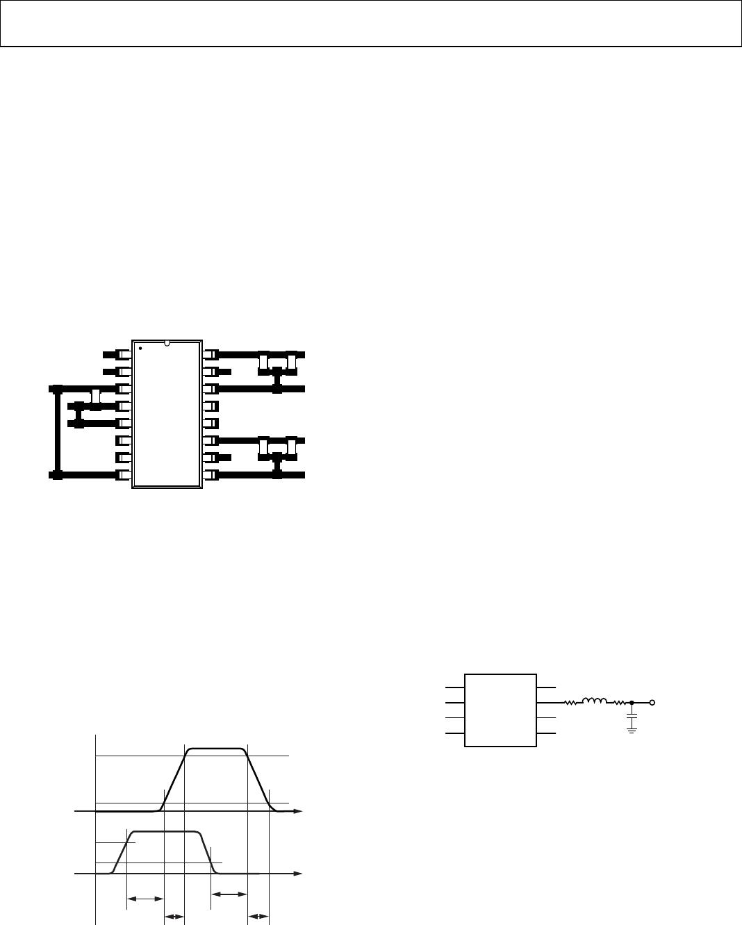
PC BOARD LAYOUT
The ADuM3223/ADuM4223 digital isolators require no external
interface circuitry for the logic interfaces. Power supply bypassing
is required at the input and output supply pins, as shown in
Figure 19. Use a small ceramic capacitor with a value between
0.01 µF and 0.1 µF to provide a good high frequency bypass.
On the output power supply pin, V
DDA
or V
DDB
, it is also recom-
mended to add a 10 µF capacitor to provide the charge required
to drive the gate capacitance at the ADuM3223/ADuM4223
outputs. On the output supply pin, the bypass capacitor use of
vias should be avoided or multiple vias should be employed to
reduce the inductance in the bypassing. The total lead length
between both ends of the smaller capacitor and the input or
output power supply pin should not exceed 5 mm.
Figure 19. Recommended PCB Layout
PROPAGATION DELAY-RELATED PARAMETERS
Propagation delay is a parameter that describes the time it takes
a logic signal to propagate through a component. The propagation
delay to a logic low output can differ from the propagation delay
to a logic high output. The ADuM3223/ADuM4223 specify t
DLH
(see Figure 20) as the time between the rising input high logic
threshold, V
IH
, to the output rising 10% threshold. Likewise, the
falling propagation delay, t
DHL
, is defined as the time between
the input falling logic low threshold, V
IL
, and the output falling
90% threshold. The rise and fall times are dependent on the
loading conditions and are not included in the propagation
delay, which is the industry standard for gate drivers.
Figure 20. Propagation Delay Parameters
Channel-to-channel matching refers to the maximum amount
that the propagation delay differs between channels within a
single ADuM3223/ADuM4223 component.
Propagation delay skew refers to the maximum amount that
the propagation delay differs between multiple ADuM3223/
ADuM4223 components operating under the same conditions.
THERMAL LIMITATIONS AND SWITCH LOAD
CHARACTERISTICS
For isolated gate drivers, the necessary separation between the
input and output circuits prevents the use of a single thermal
pad beneath the part, and heat is, therefore, dissipated mainly
through the package pins.
Package thermal dissipation limits the performance of switching
frequency vs. output load, as illustrated in Figure 7 and Figure 8
for the maximum load capacitance that can be driven with a 1 Ω
series gate resistance for different values of output voltage. For
example, this curve shows that a typical ADuM3223 can drive a
large MOSFET with 140 nC gate charge at 8 V output (which is
equivalent to a 17 nF load) up to a frequency of about 300 kHz.
Each of the ADuM3223/ADuM4223 isolator outputs has a thermal
shutdown protection function, which sets an output to a logic
low when the rising junction temperature typically reaches
150°C, and turns back on after the junction temperature falls
from the shutdown by approximately 10°C.
OUTPUT LOAD CHARACTERISTICS
The ADuM3223/ADuM4223 output signals depend on the
characteristics of the output load, which is typically an N-channel
MOSFET. The driver output response to an N-channel MOSFET
load can be modeled with a switch output resistance (R
SW
), an
inductance due to the printed circuit board trace (L
TRACE
), a series
gate resistor (R
GATE
), and a gate-to-source capacitance (C
GS
), as
shown in Figure 21.
Figure 21. RLC Model of the Gate of an N-Channel MOSFET
R
SW
is the switch resistance of the internal ADuM3223/ADuM4223
driver output, which is about 1.1 Ω. R
GATE
is the intrinsic gate
resistance of the MOSFET and any external series resistance. A
MOSFET that requires a 4 A gate driver has a typical intrinsic
gate resistance of about 1 Ω and a gate-to-source capacitance,
C
GS
, of between 2 nF and 10 nF. L
TRACE
is the inductance of the
printed circuit board trace, typically a value of 5 nH or less for a
well-designed layout with a very short and wide connection from
the ADuM3223/ADuM4223 output to the gate of the MOSFET.
10450-119
V
IA
V
DDA
V
IB
V
OA
V
DD1
GND
A
GND
1
NC
DISABLE NC
NC V
DDB
NC V
OB
V
DD1
GND
B
OUTPUT
INPUT
t
DLH
t
R
90%
10%
V
IH
V
IL
t
F
t
DHL
10450-005
ADuM3223/
ADuM4223
V
IA
V
OA
R
SW
R
GATE
C
GS
L
TRACE
V
O
10450-006