ADuM3223/ADuM4223 Data Sheet
Rev. I | Page 4 of 20
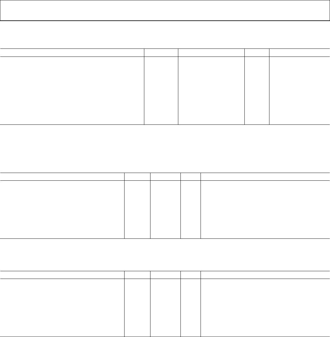
ELECTRICAL CHARACTERISTICS—3.3 V OPERATION
All voltages are relative to their respective ground. 3.0 V ≤ V
DD1
≤ 3.6 V, 4.5 V ≤ V
DD2
≤ 18 V, unless stated otherwise. All minimum/
maximum specifications apply over T
J
= −40°C to 125°C. All typical specifications are at T
J
= 25°C, V
DD1
= 3.3 V, V
DD2
= 12 V. Switching
specifications are tested with CMOS signal levels.
Table 2.
Parameter Symbol Min Typ Max Unit Test Conditions
DC SPECIFICATIONS
Input Supply Current, Quiescent I
DDI(Q)
0.87 1.4 mA
Output Supply Current, Per Channel, Quiescent I
DDO(Q)
2.3 3.2 mA
Supply Current at 1 MHz
V
DD1
Supply Current I
DD1(Q)
1.1 1.5 mA Up to 1 MHz, no load
V
DDA
/V
DDB
Supply Current I
DDA
/I
DDB(Q)
5.6 8.0 mA Up to 1 MHz, no load
Input Currents I
IA
, I
IB
−10 +0.01 +10 μA 0 V
IA
, V
IB
≤ V
DD1
Logic High Input Threshold V
IH
0.7 × V
DD1
V
Logic Low Input Threshold V
IL
0.3 × V
DD1
V
Logic High Output Voltages V
OAH
, V
OBH
V
DD2
– 0.1 V
DD2
V I
Ox
= −20 mA, V
Ix
= V
IxH
Logic Low Output Voltages V
OAL
, V
OBL
0.0 0.15 V I
Ox
= +20 mA, V
Ix
= V
IxL
Undervoltage Lockout, V
DD2
Supply
Positive Going Threshold V
DD2UV+
4.1 4.4 V A-grade
Negative Going Threshold V
DD2UV−
3.2 3.6 V A-grade
Hysteresis V
DD2UVH
0.5 V A-grade
Positive Going Threshold V
DD2UV+
6.9 7.4 V B-grade
Negative Going Threshold V
DD2UV−
5.7 6.2 V B-grade
Hysteresis V
DD2UVH
0.7 V B-grade
Positive Going Threshold V
DD2UV+
10.5 11.1 V C-grade
Negative Going Threshold V
DD2UV−
8.9 9.6 V C-grade
Hysteresis V
DD2UVH
0.9 V C-grade
Output Short-Circuit Pulsed Current
1
I
OA(SC)
, I
OB(SC)
2.0 4.0 A V
DD2
= 12 V
Output Pulsed Source Resistance R
OA
, R
OB
0.3 1.1 3.0 Ω V
DD2
= 12 V
Output Pulsed Sink Resistance R
OA
, R
OB
0.3 0.6 3.0 Ω V
DD2
= 12 V
THERMAL SHUTDOWN TEMPERATURE
Junction Temperature Shutdown, Rising Edge T
JR
150 °C
Junction Temperature Shutdown, Falling Edge T
JF
140 °C
SWITCHING SPECIFICATIONS
Pulse Width
2
PW 50 ns C
L
= 2 nF, V
DD2
= 12 V
Maximum Data Rate
3
1 MHz C
L
= 2 nF, V
DD2
= 12 V
Propagation Delay
4
t
DHL
, t
DLH
35 47 59 ns C
L
= 2 nF, V
DD2
= 12 V, see Figure 20
ADuM3223A/ADuM4223A t
DHL
, t
DLH
37 51 65 ns C
L
= 2 nF, V
DD2
= 4.5 V, see Figure 20
Propagation Delay Skew
5
t
PSK
12 ns C
L
= 2 nF, V
DD2
= 12 V, see Figure 20
Channel-to-Channel Matching
6
t
PSKCD
1 5 ns C
L
= 2 nF, V
DD2
= 12 V, see Figure 20
t
PSKCD
1 7 ns C
L
= 2 nF, V
DD2
= 4.5 V, see Figure 20
Output Rise/Fall Time (10% to 90%) t
R
/t
F
6 12 22 ns C
L
= 2 nF, V
DD2
= 12 V, see Figure 20
Dynamic Input Supply Current Per Channel I
DDI(D)
0.05 mA/Mbps V
DD2
= 12 V
Dynamic Output Supply Current Per Channel I
DDO(D)
1.65 mA/Mbps V
DD2
= 12 V
Refresh Rate f
r
1.1 Mbps
1
Short-circuit duration less than 1 μs. Average power must conform to the limit shown under the Absolute Maximum Ratings.
2
The minimum pulse width is the shortest pulse width at which the specified timing parameter is guaranteed.
3
The maximum data rate is the fastest data rate at which the specified timing parameter is guaranteed.
4
t
DLH
propagation delay is measured from the time of the input rising logic high threshold, V
IH
, to the output rising 10% level of the V
Ox
signal. t
DHL
propagation delay is
measured from the input falling logic low threshold, V
IL
, to the output falling 90% threshold of the V
Ox
signal. See Figure 20 for waveforms of propagation delay
parameters.
5
t
PSK
is the magnitude of the worst-case difference in t
DLH
and/or t
DHL
that is measured between units at the same operating temperature, supply voltages, and output
load within the recommended operating conditions. See Figure 20 for waveforms of propagation delay parameters.
6
Channel-to-channel matching is the absolute value of the difference in propagation delays between the two channels.
Data Sheet ADuM3223/ADuM4223
Rev. I | Page 5 of 20
PACKAGE CHARACTERISTICS
Table 3.
Parameter Symbol Min Typ Max Unit Test Conditions
Resistance (Input-to-Output) R
I-O
10
12
Ω
Capacitance (Input-to-Output) C
I-O
2.0 pF f = 1 MHz
Input Capacitance C
I
4.0 pF
IC Junction-to-Ambient Thermal Resistance
ADuM3223 θ
JA
76 °C/W
ADuM4223 θ
JA
45 °C/W
IC Junction-to-Case Thermal Resistance
ADuM3223 θ
JC
42 °C/W
ADuM4223 θ
JC
29 °C/W
INSULATION AND SAFETY-RELATED SPECIFICATIONS
ADuM3223
Table 4.
Parameter Symbol Value Unit Conditions
Rated Dielectric Insulation Voltage 3000 V rms 1 minute duration
Minimum External Air Gap (Clearance) L(I01) 4.0 min mm
Measured from input terminals to output terminals,
shortest distance through air
Minimum External Tracking (Creepage) L(I02) 4.0 min mm
Measured from input terminals to output terminals,
shortest distance path along body
Minimum Internal Gap (Internal Clearance) 0.017 min mm Insulation distance through insulation
Tracking Resistance (Comparative Tracking Index) CTI >400 V DIN IEC 112/VDE 0303 Part 1
Isolation Group II Material Group (DIN VDE 0110, 1/89, Table 1)
ADuM4223
Table 5.
Parameter Symbol Value Unit Conditions
Rated Dielectric Insulation Voltage 5000 V rms 1 minute duration
Minimum External Air Gap (Clearance) L(I01) 7.6 min mm
Measured from input terminals to output terminals,
shortest distance through air
Minimum External Tracking (Creepage) L(I02) 7.6 min mm
Measured from input terminals to output terminals,
shortest distance path along body
Minimum Internal Gap (Internal Clearance) 0.017 min mm Insulation distance through insulation
Tracking Resistance (Comparative Tracking Index) CTI >400 V DIN IEC 112/VDE 0303 Part 1
Isolation Group II Material Group (DIN VDE 0110, 1/89, Table 1)
ADuM3223/ADuM4223 Data Sheet
Rev. I | Page 6 of 20
REGULATORY INFORMATION
The ADuM3223 is approved or pending approval by the organizations listed in Table 6.
Table 6.
UL CSA VDE
Recognized under UL 1577
Component Recognition
Program
1
Approved under CSA Component Acceptance Notice 5A
Certified according to DIN V VDE V 0884-10
(VDE V 0884-10): 2006-12
2
Single/Protection 3000 V rms
Isolation Voltage
Basic insulation per CSA 60950-1-07 and IEC 60950-1,
380 V rms (537 V peak) maximum working voltage
Reinforced insulation, 560 V peak
File E214100 File 205078 File 2471900-4880-0001
1
In accordance with UL 1577, each ADuM3223 is proof tested by applying an insulation test voltage ≥ 3600 V rms for 1 second (current leakage detection limit = 6 μA).
2
In accordance with DIN V VDE V 0884-10, each ADuM3223 is proof tested by applying an insulation test voltage ≥ 1050 V peak for 1 second (partial discharge
detection limit = 5 pC). An asterisk (*) marking branded on the component designates DIN V VDE V 0884-10 approval.
The ADuM4223 is approved or pending approval by the organizations listed in Table 7.
Table 7.
UL CSA CQC VDE
Recognized Under
UL 1577 Component
Recognition Program
1
Approved under CSA Component
Acceptance Notice 5A
Approved under CQC11-471543-2012
Certified according to
DIN V VDE V 0884-10
(VDE V 0884-10): 2006-12
2
Single/Protection
5000 V rms Isolation
Voltage
Reinforced insulation per
CSA 60950-1-07 and IEC 60950-1,
380 V rms (537 V peak) maximum
working voltage; basic insulation
per CSA 60950-1-07 and IEC 60950-1,
760 V rms (1074 V peak) maximum
working voltage
Reinforced insulation per GB4943.1-2011,
380 V rms (537 V peak) maximum working
voltage, tropical climate, altitude ≤ 5000 m;
basic insulation per GB4943.1-2011,
600 V rms (848 V peak) maximum working
voltage, tropical climate, altitude ≤ 5000 m
Reinforced insulation,
849 V peak
File E214100 File 205078 File CQC14001108627 File 2471900-4880-0001
1
In accordance with UL 1577, each ADuM4223 is proof tested by applying an insulation test voltage ≥ 6000 V rms for 1 second (current leakage detection limit = 10 μA).
2
In accordance with DIN V VDE V 0884-10, each ADuM4223 is proof tested by applying an insulation test voltage ≥ 1592 V peak for 1 second (partial discharge
detection limit = 5 pC). An asterisk (*) marking branded on the component designates DIN V VDE V 0884-10 approval.

ADUM4223CRWZ-RL

Mfr. #:
Manufacturer:
Analog Devices Inc.
Description:
Gate Drivers 5kV RMS Prec Half- Bridge Dvr 4A Output
Lifecycle:
New from this manufacturer.
Delivery:
DHL FedEx Ups TNT EMS
Payment:
T/T Paypal Visa MoneyGram Western Union