NUD3105DMT1G

NUD3105D
http://onsemi.com
4
TYPICAL CHARACTERISTICS
V
Z
, ZENER CLAMP VOLTAGE (V)
V
GS
= 0 V
11.0
12.0
10.0
9.0
8.0
7.0
13.0
0.1 0.2 0.3 0.4 0.5 0.6 0.7 0.80
V
DS
, DRAIN TO SOURCE VOLTAGE (V)
Figure 2. Output Characteristics
V
GS
, GATETOSOURCE VOLTAGE (V)
Figure 3. Transfer Function
TEMPERATURE (°C)
Figure 4. On Resistance Variation vs. Temperature
Figure 5. R
DS(ON)
Variation with
GateToSource Voltage
Figure 6. Zener Voltage vs. Temperature
I
Z
, ZENER CURRENT (mA)
Figure 7. Zener Clamp Voltage vs. Zener Current
I
D
, DRAIN CURRENT (A)
50 25 0 25 50 75 100
1200
1000
800
600
400
200
0
125
R
DS(on)
, DRAINTOSOURCE
RESISTANCE (mW)
V
Z
, ZENER VOLTAGE (V)
50 25 0 25 50 75 100 125
I
Z
= 10 mA
I
D
= 0.25 A
V
GS
= 3.0 V
50°C
1.0 1.2 1.4 1.60.8
50
45
40
35
30
25
20
2.0
15
1.8
R
DS(on)
, DRAINTOSOURCE
RESISTANCE (W)
I
D
= 250 mA
1.0 100.1 100
V
GS
= 0 V
V
GS
= 1.0 V
I
D
, DRAIN CURRENT (A)
V
GS
= 5.0 V
V
GS
= 3.0 V
V
GS
= 2.0 V
T
J
= 25°C
10
1.0
0.1
0.01
0.001
0.0001
0.00001
0.000001
0.5 1.0 1.5 2.0 2.5 3.0 3.5 4.0 4.5 5.0
85°C
40°C
V
DS
= 0.8 V
I
D
= 0.5 A
V
GS
= 3.0 V
I
D
= 0.5 A
V
GS
= 5.0 V
V
GS
, GATETOSOURCE VOLTAGE (V)
50°C
85°C
40°C
125°C
8.20
8.18
8.16
8.14
8.12
8.10
8.08
8.06
8.04
8.02
8.00
TEMPERATURE (°C)
10
1.0
0.1
0.01
0.001
0.0001
0.00001
85°C
40°C
25°C
25°C
25°C
1000
6.0
NUD3105D
http://onsemi.com
5
TYPICAL CHARACTERISTICS
V
DS
, DRAINTOSOURCE VOLTAGE (V)
0.01 100100.1
0.1
1.0
0.01
I
D
, DRAIN CURRENT (A)
1.0
R
DS(on)
LIMIT
THERMAL LIMIT
PACKAGE LIMIT
I
D
, DRAIN CURRENT (A)
Figure 8. OnResistance vs. Drain Current and
Temperature
TEMPERATURE (°C)
Figure 9. Gate Leakage vs. Temperature
R
DS(ON)
, DRAINTOSOURCE
RESISTANCE (W)
1.0
0.9
0.8
0.5
0.6
0.7
1.1
1.2
0.05 0.1 0.15 0.2 0.25 0.3 0.35 0.4 0.45 0.5
I
GSS
, GATE LEAKAGE (mA)
30
25
0
5
10
35
40
50 25
0
25 50 75 100 125
20
15
125°C
85°C
50°C
25°C
40°C
V
GS
= 3.0 V
V
GS
= 5.0 V
Figure 10. Safe Operating Area for NUD3105DLT1
Figure 11. Transient Thermal Response for NUD3105DLT1
0.01 0.1 1.0 10 100 1000 10,000 100,000 1,000,000
D = 0.5
0.2
0.1
0.05
0.02
SINGLE PULSE
0.01
P
d(pk)
t
1
t
2
DUTY CYCLE = t
1
/t
2
PERIOD
PW
r(t), TRANSIENT THERMAL
RESISTANCE (NORMALIZED)
1.0
0.1
0.01
0.001
t1, PULSE WIDTH (ms)
DC
PW = 0.1 s
DC = 50%
PW = 7.0 ms
DC = 5%
PW = 10 ms
DC = 20%
Typical
I
Z
vs. V
Z
V
(BR)DSS
min = 6.0 V
I
DContinuous
= 0.5 A
V
GS
= 3.0 V, T
C
= 25°C
NUD3105D
http://onsemi.com
6
Designing with this Data Sheet
1. Determine the maximum inductive load current (at
max V
CC
, min coil resistance & usually minimum
temperature) that the NUD3105D will have to
drive and make sure it is less than the max rated
current.
2. For pulsed operation, use the Transient Thermal
Response of Figure 11 and the instructions with it
to determine the maximum limit on transistor
power dissipation for the desired duty cycle and
temperature range.
3. Use Figures 10 and 11 with the SOA notes to
insure that instantaneous operation does not push
the device beyond the limits of the SOA plot.
4. Verify that the circuit driving the gate will meet
the V
GS(th)
from the Electrical Characteristics
table.
5. Using the max output current calculated in step 1,
check Figure 7 to insure that the range of Zener
clamp voltage over temperature will satisfy all
system & EMI requirements.
6. Use I
GSS
and I
DSS
from the Electrical
Characteristics table to insure that “OFF” state
leakage over temperature and voltage extremes
does not violate any system requirements.
7. Review circuit operation and insure none of the
device max ratings are being exceeded.
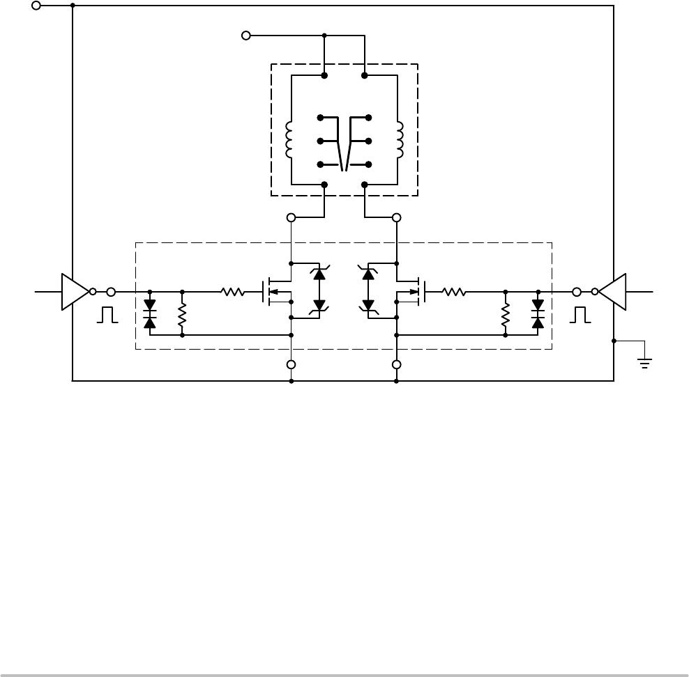
Figure 12. A 200 mW, 5.0 V Dual Coil Latching Relay Application
with 3.0 V Level Translating Interface
+4.5 V
CC
+5.5 Vdc
+
V
out
(6)
+
V
in
(2)
GND (1)
NUD3105DDMT1
+3.0 V
DD
+3.75 Vdc
APPLICATIONS DIAGRAMS
V
out
(3)
V
in
(5)
GND (4)

NUD3105DMT1G

Mfr. #:
Manufacturer:
ON Semiconductor
Description:
Gate Drivers 5V Dual Integrated Relay Inductive Load
Lifecycle:
New from this manufacturer.
Delivery:
DHL FedEx Ups TNT EMS
Payment:
T/T Paypal Visa MoneyGram Western Union

Products related to this Datasheet