©2011 Silicon Storage Technology, Inc. DS25028A 08/11
22
16 Mbit / 32 Mbit Multi-Purpose Flash Plus
SST39VF1601 / SST39VF3201
SST39VF1602 / SST39VF3202
Not Recommended for New Designs
A
Microchip Technology Company
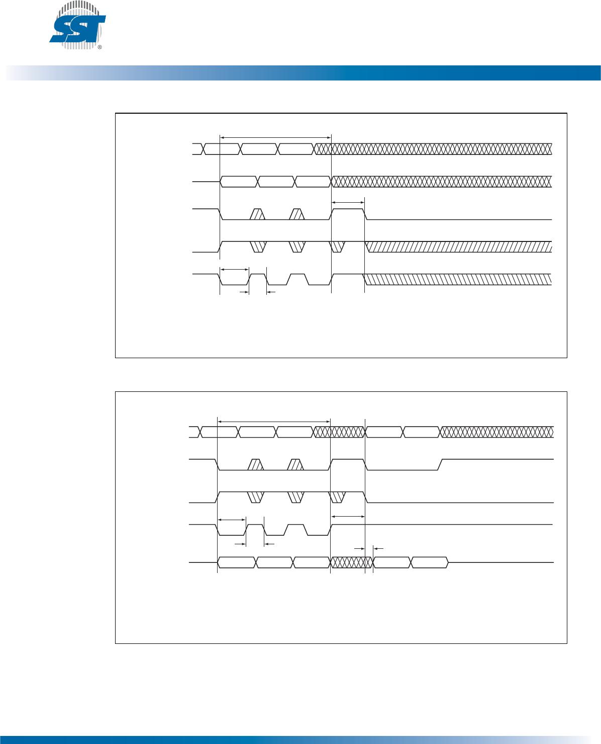
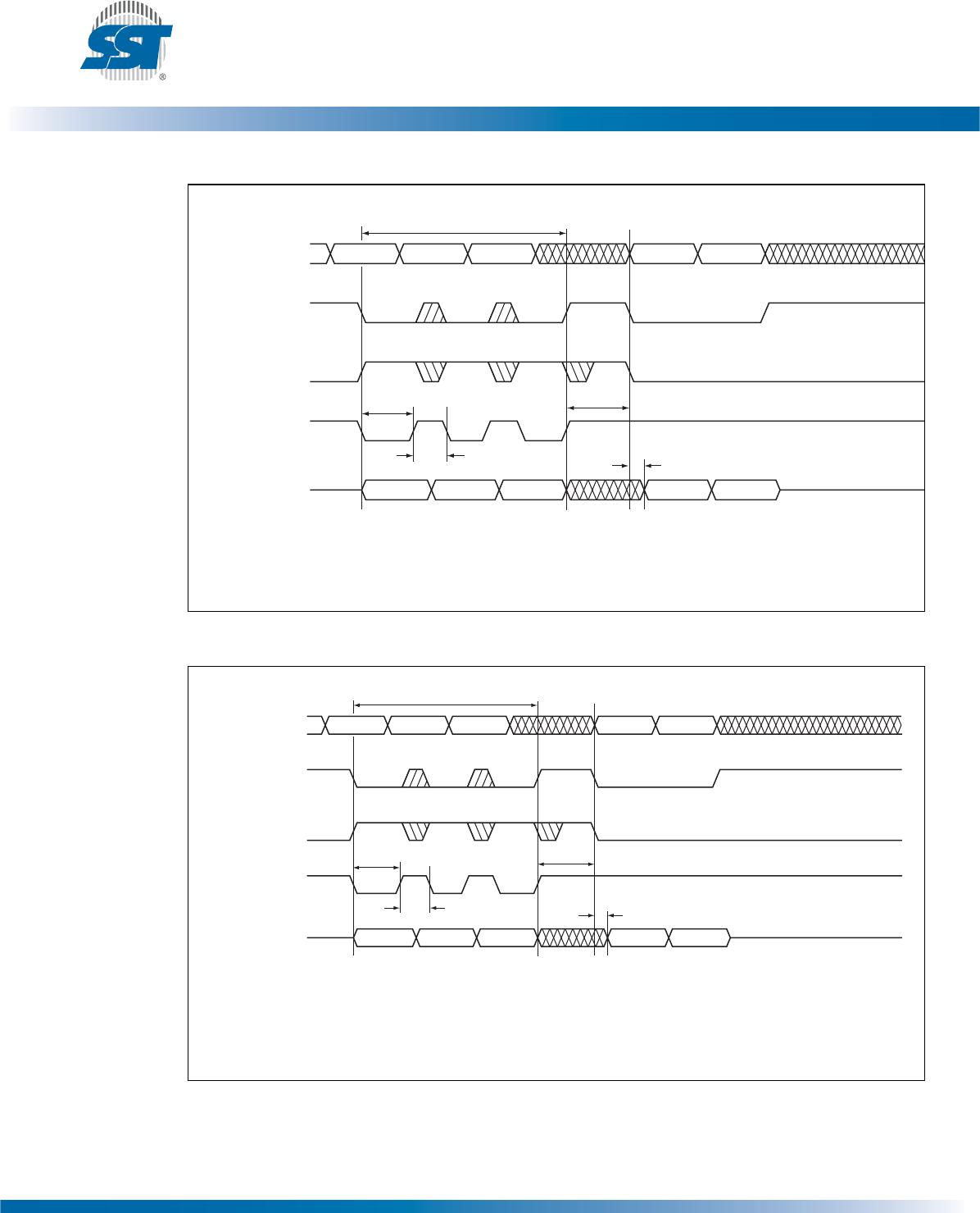
Figure 12:Software ID Entry and Read
Figure 13:CFI Query Entry and Read
1
ADDRESS A
14-0
T
IDA
DQ
15-0
WE#
SW0 SW1 SW2
5555 2AAA 5555 0000 0001
OE#
CE#
Three-Byte Sequence for Software ID Entry
T
WP
T
WPH
T
AA
00BF
Device IDXX55XXAA XX90
Note: Device ID = 234BH for 39VF1601, 234AH for 39VF1602, 235BH for 39VF3201, and 235AH for 39VF3202,
WP# must be held in proper logic state (V
IL
or V
IH
) 1 µs prior to and 1 µs after the command sequence
X can be V
IL
or V
IH,
but no other value
1223 F12.1
ADDRESS A
14-0
T
IDA
DQ
15-0
WE#
SW0 SW1 SW2
5555 2AAA 5555
OE#
CE#
Three-Byte Sequence for CFI Query Entry
T
WP
T
WPH
T
AA
XX55XXAA XX98
Note: WP# must be held in proper logic state (V
IL
or V
IH
) 1 µs prior to and 1 µs after the command sequence
X can be V
IL
or V
IH
,
but no other value
©2011 Silicon Storage Technology, Inc. DS25028A 08/11
23
16 Mbit / 32 Mbit Multi-Purpose Flash Plus
SST39VF1601 / SST39VF3201
SST39VF1602 / SST39VF3202
Not Recommended for New Designs
A
Microchip Technology Company
Figure 14:Software ID Exit/CFI Exit
Figure 15:SecIDEntry
1223 F13.0
ADDRESS A
14-0
DQ
15-0
T
IDA
T
WP
T
WHP
WE#
SW0 SW1 SW2
5555 2AAA 5555
THREE-BYTE SEQUENCE FOR
SOFTWARE ID EXIT AND RESET
OE#
CE#
XXAA XX55 XXF0
Note: WP# must be held in proper logic state (V
IL
or V
IH
) 1 µs prior to and 1 µs after the command sequence
X can be V
IL
or V
IH,
but no other value
1223 F20.2
ADDRESS A
MS-0
T
IDA
DQ
15-0
WE#
SW0 SW1 SW2
5555 2AAA 5555
OE#
CE#
THREE-BYTE SEQUENCE FOR
CFI QUERY ENTRY
T
WP
T
WPH
T
AA
XX55XXAA XX88
Note: A
MS
= Most significant address
A
MS
=A
19
for SST39VF1601/1602 and A
20
for SST39VF3201/3202
WP# must be held in proper logic state (V
IL
or V
IH
) 1 µs prior to and 1 µs after the command sequence
X can be V
IL
or V
IH,
but no other value.
©2011 Silicon Storage Technology, Inc. DS25028A 08/11
24
16 Mbit / 32 Mbit Multi-Purpose Flash Plus
SST39VF1601 / SST39VF3201
SST39VF1602 / SST39VF3202
Not Recommended for New Designs
A
Microchip Technology Company
Figure 16:RST# Timing Diagram (When no internal operation is in progress)
Figure 17:RST# Timing Diagram (During Program or Erase operation)
Figure 18:AC Input/Output Reference Waveforms
Figure 19:A Test Load Example
1223 F22.1
RST#
CE#/OE#
T
RP
T
RHR
1223 F23.0
RST#
CE#/OE#
T
RP
T
RY
End-of-Write Detection
(Toggle-Bit)
1223 F14.0
REFERENCE POINTS OUTPUTINPUT
V
IT
V
IHT
V
ILT
V
OT
AC test inputs are driven at V
IHT
(0.9 V
DD
) for a logic “1” and V
ILT
(0.1 V
DD
) for a
logic “0”. Measurement reference points for inputs and outputs are V
IT
(0.5 V
DD
) and V
OT
(0.5
V
DD
). Input rise and fall times (10% 90%) are <5 ns.
Note: V
IT
-V
INPUT
Test
V
OT
-V
OUTPUT
Test
V
IHT
-V
INPUT
HIGH Test
V
ILT
-V
INPUT
LOW Test
1223 F15.0
TO TESTER
TO DUT
C
L

SST39VF3201-70-4C-B3KE-T

Mfr. #:
Manufacturer:
Microchip Technology
Description:
NOR Flash 32M (2Mx16) 70ns 2.7-3.6V Commercial
Lifecycle:
New from this manufacturer.
Delivery:
DHL FedEx Ups TNT EMS
Payment:
T/T Paypal Visa MoneyGram Western Union