1
JUNE 2012
CMOS ASYNCHRONOUS FIFO
256 x 9, 512 x 9 and 1,024 x 9
IDT7200L
IDT7201LA
IDT7202LA
IDT and the IDT logo are registered trademarks of Integrated Device Technology, Inc.
COMMERCIAL, INDUSTRIAL AND MILITARY TEMPERATURE RANGES
©2012 Integrated Device Technology, Inc. All rights reserved. Product specifications subject to change without notice. DSC-2679/14
FEATURES:
First-In/First-Out dual-port memory
256 x 9 organization (IDT7200)
512 x 9 organization (IDT7201)
1,024 x 9 organization (IDT7202)
Low power consumption
— Active: 440mW (max.)
—Power-down: 28mW (max.)
Ultra high speed—12ns access time
Asynchronous and simultaneous read and write
Fully expandable by both word depth and/or bit width
720x family is pin and functionally compatible from 256 x 9 to 64k x 9
Status Flags: Empty, Half-Full, Full
Auto-retransmit capability
High-performance CEMOS™ technology
Military product compliant to MIL-STD-883, Class B
Standard Military Drawing #5962-87531, 5962-89666, 5962-89863
and 5962-89536 are listed on this function
Dual versions available in the TSSOP package. For more informa-
tion, see IDT7280/7281/7282 data sheet
IDT7280 = 2 x IDT7200
IDT7281 = 2 x IDT7201
IDT7282 = 2 x IDT7202
DESCRIPTION:
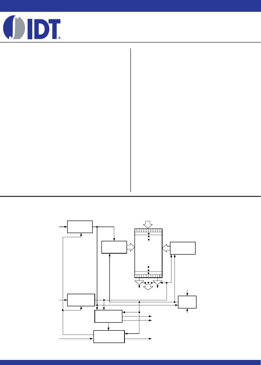
The IDT7200/7201/7202 are dual-port memories that load and empty data
on a first-in/first-out basis. The devices use Full and Empty flags to prevent data
overflow and underflow and expansion logic to allow for unlimited expansion
capability in both word size and depth.
The reads and writes are internally sequential through the use of ring
pointers, with no address information required to load and unload data. Data
is toggled in and out of the devices through the use of the Write (W) and Read
(R) pins.
The devices utilize a 9-bit wide data array to allow for control and parity bits
at the user’s option. This feature is especially useful in data communications
applications where it is necessary to use a parity bit for transmission/reception
error checking. It also features a Retransmit (RT) capability that allows for reset
of the read pointer to its initial position when RT is pulsed LOW to allow for
retransmission from the beginning of data. A Half-Full Flag is available in the
single device mode and width expansion modes.
These FIFOs are fabricated using high-speed CMOS technology. They
are designed for those applications requiring asynchronous and simultaneous
read/writes in multiprocessing and rate buffer applications. Military grade
product is manufactured in compliance with MIL-STD-883, Class B.
FUNCTIONAL BLOCK DIAGRAM
W
WRITE
CONTROL
READ
CONTROL
R
FLAG
LOGIC
EXPANSION
LOGIC
XI
WRITE
POINTER
RAM
ARRAY
256 x 9
512 x 9
1,024 x 9
READ
POINTER
DATA INPUTS
RESET
LOGIC
THREE-
STATE
BUFFERS
DATA OUTPUTS
EF
FF
XO/HF
RS
FL/RT
(D
0
-D
8
)
2679 drw 01
(Q
0
-Q
8
)
Industrial temperature range (–40
o
C to +85
o
C) is available
(plastic packages only)
Green parts available, see ordering information
2
COMMERCIAL, INDUSTRIAL AND MILITARY
TEMPERATURE RANGES
IDT7201L/7201LA/7202LA CMOS ASYNCHRONOUS FIFO
256 x 9, 512 x 9 and 1,024 x 9
PIN CONFIGURATIONS
RECOMMENDED DC OPERATING
CONDITIONS
Symbol Parameter Min. Typ. Max. Unit
V
CC Supply Voltage 4.5 5.0 5.5 V
Commercial/Industrial/Military
GND Supply Voltage 0 0 0 V
VIH
(1)
Input High Voltage Com'l/Ind'l 2.0 V
VIH
(1)
Input High Voltage Military 2.2 V
V
IL
(2)
Input Low Voltage 0.8 V
Commercial/Industrial/Military
TA Operating Temperature Commercial 0 70 ° C
TA Operating Temperature Industrial 40 85 ° C
T
A Operating Temperature Military 55 125 ° C
NOTES:
1. For RT/RS/XI input, VIH = 2.6V (commercial).
For RT/RS/XI input, VIH = 2.8V (military).
2. 1.5V undershoots are allowed for 10ns once per cycle.
ABSOLUTE MAXIMUM RATINGS
Symbol Rating Com’l & Ind'l Mil. Unit
VTERM Terminal Voltage –0.5 to +7.0 –0.5 to +7.0 V
with Respect
to GND
TSTG Storage –55 to +125 –65 to +155 ° C
Temperature
I
OUT DC Output –50 to +50 –50 to +50 mA
Current
NOTE:
1. Stresses greater than those listed under ABSOLUTE MAXIMUM RATINGS may cause
permanent damage to the device. This is a stress rating only and functional operation of
the device at these or any other conditions above those indicated in the operational
sections of this specification is not implied. Exposure to absolute maximum rating
conditions for extended periods may affect reliability.
Reference Order
Package Type Identifier Code
PLASTIC DIP
(1)
P28-1 P
PLASTIC THIN DIP P28-2 TP
CERDIP
(1)
D28-1 D
THIN CERDIP D28-3 TD
SOIC SO28-3 SO
TOP VIEW
Reference Order
Package Type Identifier Code
LCC
(1)
L32- 1 L
PLCC J32-1 J
TOP VIEW
NOTE:
1. The 600-mil-wide DIP (P28-1 and D28-1) and LCC are not available for the IDT7200.
W
D8
VCC
D4
1
2
28
27
D3 D5326
D2 D6425
D1 D7524
D0 FL/RT623
XI RS
722
FF EF
821
Q0 XO/HF920
Q1 Q710 19
Q2 Q611 18
Q3 Q512 17
Q8 Q413 16
GND
R
14 15
2679 drw 02a
D
2
5
D
1
6
D
0
7
XI
8
FF
9
Q
0
10
Q
1
11
NC 12
Q
2
13
D
6
D
7
NC
FL/RT
RS
EF
XO/HF
Q
7
Q
6
29
28
27
26
25
24
23
22
21
4
3 2
1
32 31 30
14 15 16 17 18 19 20
Q
3
Q
8
GND
NC
R
Q
4
Q
5
D
3
D
8
W
NC
V
CC
D
4
D
5
INDEX
2679 drw 02b
3
COMMERCIAL, INDUSTRIAL AND MILITARY
TEMPERATURE RANGES
IDT7201L/7201LA/7202LA CMOS ASYNCHRONOUS FIFO
256 x 9, 512 x 9 and 1,024 x 9
DC ELECTRICAL CHARACTERISTICS
(Commercial: VCC = 5V ± 10%, TA = 0
o
C to +70
o
C; Industrial: VCC = 5V ± 10%, TA = –40
o
C to +85
o
C; Military: VCC = 5V ± 10%, TA = –55
o
C to +125
o
C)
IDT7200L IDT7200L
IDT7201LA IDT7201LA
IDT7202LA IDT7202LA
Com'l & Ind'l
(1)
Military
(2)
tA = 12, 15, 20, 25, 35, 50 ns tA = 20, 30, 50, 80 ns
Symbol Parameter Min. Max. Min. Max. Unit
I
LI
(3)
Input Leakage Current (Any Input) 1 1 10 10 μA
I
LO
(4)
Output Leakage Current 10 10 10 10 μA
V
OH Output Logic “1” Voltage IOH = –2mA 2.4 2.4 V
V
OL Output Logic “0” Voltage IOL = 8mA 0.4 0.4 V
I
CC1
(5,6,7)
Active Power Supply Current 80 100 mA
ICC2
(5,8)
Standby Current (R=W=RS=FL/RT=VIH)—515mA
NOTES:
1. Industrial temperature range product for the 15ns and 25 ns speed grades are available as a standard device.
2. Military speed grades of 50ns and 80ns are only available for the IDT7201LA.
3. Measurements with 0.4 V
IN VCC.
4. R V
IH, 0.4 VOUT VCC.
5. Tested with outputs open (IOUT = 0).
6. Tested at f = 20 MHz.
7. Typical ICC1 = 15 + 2*fS + 0.02*CL*fS (in mA) with VCC = 5V, TA = 25°C, fS = WCLK frequency = RCLK frequency (in MHz, using TTL levels), data switching at fS/2, CL = capacitive
load (in pF).
8. All Inputs = VCC - 0.2V or GND + 0.2V.
AC TEST CONDITIONS
Input Pulse Levels GND to 3.0V
Input Rise/Fall Times 5ns
Input Timing Reference Levels 1.5V
Output Reference Levels 1.5V
Output Load See Figure 1
Symbol Parameter Condition Max. Unit
C
IN Input Capacitance VIN = 0V 8 pF
COUT Output Capacitance VOUT = 0V 8 pF
NOTE:
1. Characterized values, not currently tested.
CAPACITANCE (TA = +25°C, f = 1.0 MHz)
or equivalent circuit
2679 drw 03
30pF*
1.1K
5V
TO
OUTPUT
PIN
680Ω
Figure 1. Output Load
* Includes scope and jig capacitances.

7200L20TDB

Mfr. #:
Manufacturer:
IDT
Description:
FIFO 256 X 9 CMOS PARALLEL FIF
Lifecycle:
New from this manufacturer.
Delivery:
DHL FedEx Ups TNT EMS
Payment:
T/T Paypal Visa MoneyGram Western Union