CD214A-B240LF

Features
RoHS compliant*
SMA package
Surface mount
Very low forward voltage drop
CD214A-B220 ~ B260 Schottky Barrier Rectifi er Chip Diode
*RoHS Directive 2002/95/EC Jan. 27, 2003 including annex and RoHS Recast
2011/65/EU June 8, 2011.
Specifi cations are subject to change without notice.
The device characteristics and parameters in this data sheet can and do vary in different
applications and actual device performance may vary over time.
Users should verify actual device performance in their specifi c applications.
General Information
The markets of portable communications, computing and video equipment are challenging the semiconductor industry to develop increasingly
smaller electronic components.
Bourns offers Schottky Rectifi er Diodes for rectifi cation applications, in compact chip package DO-214AC (SMA) size format, which offer PCB
real estate savings and are considerably smaller than competitive parts. The Schottky Rectifi er Diodes offer a forward current of 2 A with a
choice of repetitive peak reverse voltage of 20 V up to 60 V.
Bourns
®
Chip Diodes conform to JEDEC standards, are easy to handle on standard pick and place equipment and their fl at confi guration
minimizes roll away.
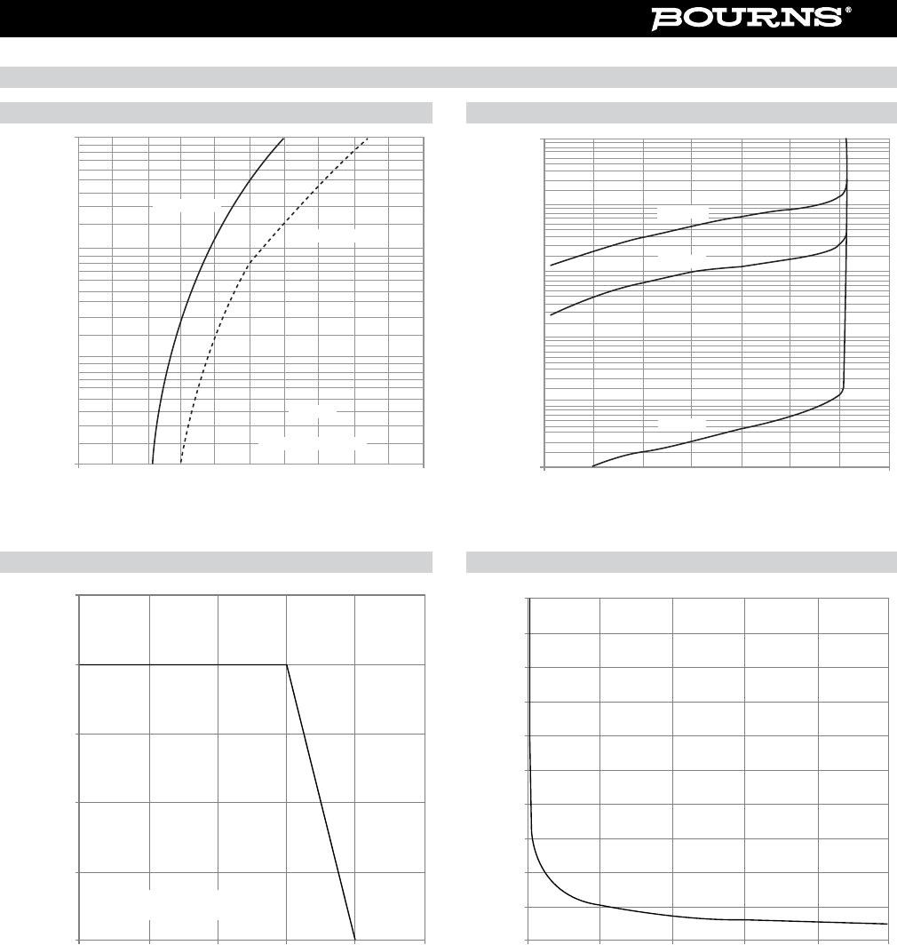
Electrical Characteristics (@ T
A
= 25 °C Unless Otherwise Noted)
Parameter Symbol
CD214A-
Unit
B220 B230 B240 B240L B250 B260
Forward Voltage (Max.)
(l
f
= 2 A)
V
F
0.5 0.5 0.5 0.43 0.7 0.7 V
Typical Junction
Capacitance**
C
T
200 pF
Reverse Current (Max.)
at Rated V
R
)
I
R
0.5 0.5 0.5 2.0 0.5 0.5 mA
*RoHS COMPLIANT
** Measured at 1.0 MHz and applied reverse voltage of 4.0 VDC.
Absolute Ratings (@ T
A
= 25 °C Unless Otherwise Noted)
Parameter Symbol
CD214A-
Unit
B220 B230 B240 B240L B250 B260
Repetitive Peak
Reverse Voltage
V
RRM
20 30 40 40 50 60 V
Reverse Voltage V
R
20 30 40 40 50 60 V
Maximum RMS Voltage V
RMS
14 21 28 28 35 42 V
Avg. Forward Current I
O
2A
Forward Current,
Surge Peak
(60 Hz, 1 cycle)
I
surge
50 50 50 25 50 50 A
Typical Thermal
Resistance***
R
ƟJL
15 15 15 18 15 15 °C/W
Storage Temperature T
STG
-55 to +150 °C
Junction Temperature T
J
-55 to +125 °C
*** Thermal resistance junction to lead.
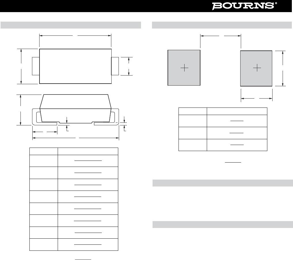
How to Order
CD 214A - B 2 40 L LF
Common Code
Chip Diode
Package
214A = SMA/DO-214AC
Model
B = Schottky Barrier Series
Average Forward Current (I
O
) Code
2 = 2 A (Code x 1000 mA = Average Forward Current)
Reverse Voltage (VR) Code
30 = 30 V
40 = 40 V
60 = 60 V
Forward Voltage Suffi x (Applies to -B240L only)
L = Low Forward Voltage V
f
(-B240L only)
No Space in P/N = Not Low Forward Voltage
Terminations
LF = 100 % Sn (RoHS Compliant*)
Asia-Pacifi c: Tel: +886-2 2562-4117 • Fax: +886-2 2562-4116
EMEA: Tel: +36 88 520 390 • Fax: +36 88 520 211
The Americas: Tel: +1-951 781-5500 • Fax: +1-951 781-5700
www.bourns.com
Specifi cations are subject to change without notice.
The device characteristics and parameters in this data sheet can and do vary in different applications and actual device performance may vary over time.
Users should verify actual device performance in their specifi c applications.
CD214A-B220 ~ B260 Schottky Barrier Rectifi er Chip Diode
Product Dimensions Recommended Pad Layout
Physical Specifi cations
Case ...........................................................................Molded plastic
Polarity.................................................... Indicated by cathode band
Weight .................................................. 0.002 ounces / 0.064 grams
DIMENSIONS:
MM
(INCHES)
Dimension SMA (DO-214AC)
A
4.06 - 4.57
(0.160 - 0.180)
B
2.29 - 2.92
(0.090 - 0.115)
C
1.27 - 1.63
(0.050 - 0.064)
D
0.15 - 0.31
(0.006 - 0.110)
E
4.83 - 5.59
(0.190 - 0.220)
F
0.05 - 0.20
(0.002 - 0.008)
G
2.01 - 2.62
(0.080 - 0.103)
H
0.76 - 1.52
(0.030 - 0.060)
Dimension SMA (DO-214AC)
A
2.90
(0.114)
B
2.40
(0.094)
C
2.30
(0.091)
DIMENSIONS:
MM
(INCHES)
Typical Part Marking
CD214A-B220 .....................................................................B 220A
CD214A-B230 .....................................................................B 230A
CD214A-B240 .....................................................................B 240A
CD214A-B240L ...................................................................B 240LA
CD214A-B250 .....................................................................B 250A
CD214A-B260 .....................................................................B 260A
B
G
F D
C
H
E
A
A
C
B
0.1
1
10
0.01
Forward Current (Amps)
0.0
0.2
0.4 0.6 0.8 1.0
Forward Voltage (Volts)
Tj=25 °C
PULSEWIDTH 300μs
B220 to B240
B250 to B260
100
0.1
1
10
0.001
0.01
Reverse Current (mAmps)
0
20
40 60 80 100 140
Percent of Rated Peak Reverse Voltage (%)
120
Tj=25 °C
Tj=100 °C
Tj=125 °C
Specifi cations are subject to change without notice.
The device characteristics and parameters in this data sheet can and do vary in different applications and actual device performance may vary over time.
Users should verify actual device performance in their specifi c applications.
CD214A-B220 ~ B260 Schottky Barrier Rectifi er Chip Diode
Rating and Characteristic Curves: CD214A-B220, CD214A-B230, CD214A-B240, CD214A-B250 & CD214A-B260
Forward Characteristics Reverse Characteristics
Derating Curve Capacitance Between Terminals
2.50
2.00
1.50
1.00
0.50
0.00
25 50 75 100 125 150
Average Forward Current (Amps)
Lead Tem
p
erature
(
°C
)
Single Phase Half Wave 60 Hz
Resistive or Inductive Load
1000
100
200
300
400
500
600
700
800
900
0
020406080100
Capacitance (pF)
Reverse Voltage (Volts)
F = 1 MHz
Ta = 25 °C

CD214A-B240LF

Mfr. #:
Manufacturer:
Bourns
Description:
Schottky Diodes & Rectifiers 2A 40V
Lifecycle:
New from this manufacturer.
Delivery:
DHL FedEx Ups TNT EMS
Payment:
T/T Paypal Visa MoneyGram Western Union