gDDR3 SDRAM Graphics Addendum
MT41J256M16 – 32 Meg x 16 x 8 Banks
Features
• V
DD
= V
DDQ
= +1.5V (1.425–1.575V)
• V
DD
= V
DDQ
= +1.35V (1.283–1.45V) capable at down
clocked speeds
• Differential bidirectional data strobe
• 8n-bit prefetch architecture
• Differential clock inputs (CK, CK#)
• 8 internal banks
• Nominal and dynamic on-die termination (ODT)
for data, strobe, and mask signals
• Programmable CAS READ latency (CL)
• Posted CAS additive latency (AL): 0, CL - 1, CL - 2
• Programmable CAS WRITE latency (CWL)
• Fixed burst length (BL) of 8 and burst chop (BC) of 4
(via the mode register set [MRS])
• Selectable BC4 or BL8 on-the-fly (OTF)
• Self refresh mode
• T
C
of 0°C to 115°C
– 64ms, 8192 cycle refresh at 0°C to 85°C
– 32ms at 85°C to 115°C
• Self refresh temperature (SRT)
• Automatic self refresh (ASR)
• Write leveling
• Multipurpose register
• Output driver calibration
Options Marking
• Configuration
– 256 Meg x 16 256M16
• FBGA package (Pb-free) – x16
– 96-ball (7.5mm x 13.5mm) LY
• Timing – cycle time
– 1.0ns @ CL = 14 (gDDR3-2000) -091G
• Operating temperature
– Commercial (0°C ≤ T
C
≤ 115°C) None
• Revision :N
Note:
1. For complete device functionality and speci-
fications, refer to the standard 4Gb DDR3
SDRAM data sheet found at www.mi-
cron.com. The information in this data
sheet supersedes the standard data sheet.
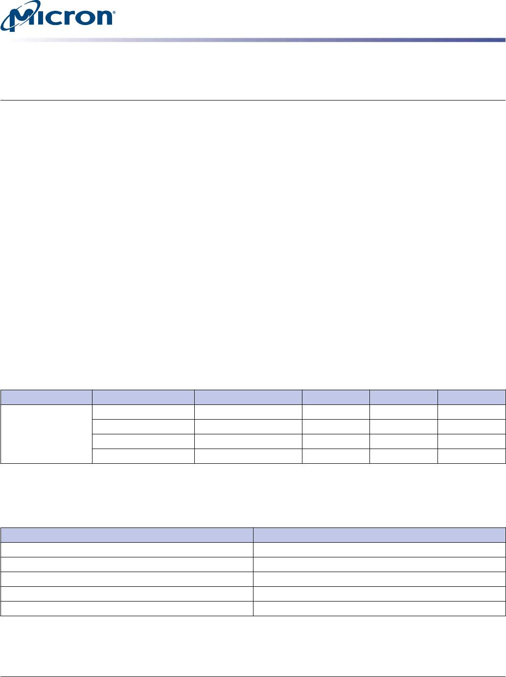
Table 1: Key Timing Parameters
Speed Grade Data Rate (MT/s) Target
t
RCD-
t
RP-CL
t
RCD (ns)
t
RP (ns) CL (ns)
-091G
2200
1
15-15-15 13.65 13.65 13.65
2000
2
14-14-14 14 14 14
1800
2
13-13-13 14.3 14.3 14.3
1600
2
11-11-11 13.75 13.75 13.75
Notes:
1. Requires V
DD
= V
DDQ
= +1.5V
NOM
2. V
DD
= V
DDQ
= +1.35V
NOM
capable
Table 2: Addressing
Parameter 256 Meg x 16
Configuration 32 Meg x 16 x 8 banks
Refresh count 8K
Row addressing 32K (A[14:0])
Bank addressing 8 (BA[2:0])
Column addressing 1K (A[9:0])
4Gb: x16 gDDR3 SDRAM Graphics Addendum
Features
CCMTD-1005363231-10344
ddr3_4gb_graphics_addendum 091.pdf - Rev. A 05/16 EN
1
Micron Technology, Inc. reserves the right to change products or specifications without notice.
© 2012 Micron Technology, Inc. All rights reserved.
Products and specifications discussed herein are subject to change by Micron without notice.