Package Dimensions
Figure 2: 96-Ball FBGA – x16 (LY)
Seating plane
0.12 A
Ball A1 ID
(covered by SR)
Ball A1 ID
A
0.34 ±0.05
1.1 ±0.1
6.4 CTR
7.5 ±0.1
0.8 TYP
12 CTR
13.5 ±0.1
96X Ø0.47
Dimensions apply
to solder balls post-
reflow on Ø0.42
SMD ball pads.
0.8 TYP
1.8 CTR
Nonconductive
overmold
0.155
123789
A
B
C
D
E
F
G
H
J
K
L
M
N
P
R
T
Note:
1. All dimensions are in millimeters.
4Gb: x16 gDDR3 SDRAM Graphics Addendum
Package Dimensions
CCMTD-1005363231-10344
ddr3_4gb_graphics_addendum 091.pdf - Rev. A 05/16 EN
4
Micron Technology, Inc. reserves the right to change products or specifications without notice.
© 2012 Micron Technology, Inc. All rights reserved.
Electrical Specifications
Table 4: DC Electrical Characteristics and Operating Conditions
All voltages are referenced to V
SS
Parameter/Condition Symbol Min Nom Max Unit Notes
Supply voltage V
DD
1.425 1.5 1.575 V 1, 2, 3
I/O supply voltage V
DDQ
1.425 1.5 1.575 V 1, 2, 3
Supply voltage V
DD
1.283 1.35 1.45 V 1, 2, 4
I/O supply voltage V
DDQ
1.283 1.35 1.45 V 1, 2, 4
Notes:
1. V
DD
and V
DDQ
must track one another. V
DDQ
must be V
DD
. V
SS
= V
SSQ
.
2. V
DD
and V
DDQ
may include AC noise of ±50mV (250 kHz to 20 MHz) in addition to the
DC (0 Hz to 250 kHz) specifications. V
DD
and V
DDQ
must be at same level for valid AC
timing parameters.
3. Valid with all speed bins.
4. Not for use with -093 speed bin.
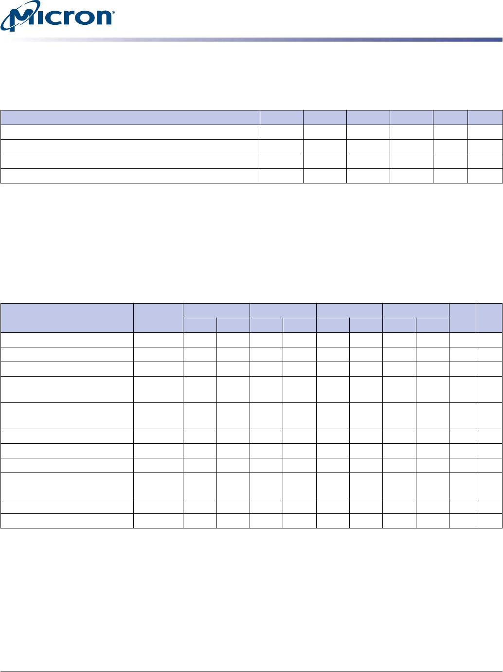
Table 5: Input/Output Capacitance
Note 1 applies to the entire table
Capacitance
Parameters Symbol
gDDR3-1600 gDDR3-1800 gDDR3-2000 gDDR3-2200
Unit
Note
sMin Max Min Max Min Max Min Max
CK and CK# C
CK
0.8 1.4 0.8 1.3 0.8 1.3 0.8 1.3 pF
ΔC: CK to CK# C
DCK
0 0.15 0 0.15 0 0.15 0 0.15 pF
Single-end I/O: DQ, DM C
IO
1.5 2.3 1.5 2.2 1.5 2.1 1.5 2.1 pF 2
Differential I/O: DQS, DQS#,
TDQS, TDQS#
C
IO
1.5 2.3 1.5 2.2 1.5 2.1 1.5 2.1 pF 3
ΔC: DQS to DQS#, TDQS,
TDQS#
C
DDQS
0 0.15 0 0.15 0 0.15 0 0.15 pF 3
ΔC: DQ to DQS C
DIO
–0.5 0.3 –0.5 0.3 –0.5 0.3 –0.5 0.3 pF 4
Inputs (CTRL, CMD, ADDR) C
I
0.75 1.3 0.75 1.2 0.75 1.2 0.75 1.2 pF 5
ΔC: CTRL to CK C
DI_CTRL
–0.4 0.2 –0.4 0.2 –0.4 0.2 –0.4 0.2 pF 6
ΔC: CMD_ADDR to CK C
DI_CMD_AD
DR
–0.4 0.4 –0.4 0.4 –0.4 0.4 –0.4 0.4 pF 7
ZQ pin capacitance C
ZO
3.0 3.0 3.0 3.0 pF
Reset pin capacitance C
RE
3.0 3.0 3.0 3.0 pF
Notes:
1. V
DD
= +1.5V ±0.075mV, V
DDQ
= V
DD
, V
REF
= V
SS
, f = 100 MHz, T
C
= 25°C. V
OUT(DC)
= 0.5 ×
V
DDQ
, V
OUT
= 0.1V (peak-to-peak).
2. DM input is grouped with I/O pins, reflecting the fact that they are matched in loading.
3. Includes TDQS, TDQS#. C
DDQS
is for DQS vs. DQS# and TDQS vs. TDQS# separately.
4. C
DIO
= C
IO(DQ)
- 0.5 × (C
IO(DQS)
+ C
IO(DQS#)
).
5. Excludes CK, CK#; CTRL = ODT, CS#, and CKE; CMD = RAS#, CAS#, and WE#; ADDR =
A[n:0], BA[2:0].
6. C
DI_CTRL
= C
I(CTRL)
- 0.5 × (C
CK(CK)
+ C
CK(CK#)
).
7. C
DI_CMD_ADDR
= C
I(CMD_ADDR)
- 0.5 × (C
CK(CK)
+ C
CK(CK#)
).
4Gb: x16 gDDR3 SDRAM Graphics Addendum
Electrical Specifications
CCMTD-1005363231-10344
ddr3_4gb_graphics_addendum 091.pdf - Rev. A 05/16 EN
5
Micron Technology, Inc. reserves the right to change products or specifications without notice.
© 2012 Micron Technology, Inc. All rights reserved.
Electrical Characteristics – I
DD
Specifications
I
DD
values are for full operating range of voltage and temperature unless otherwise no-
ted.
Table 6: I
DD
Maximum Limits - Die Rev. N
Speed Bin
gDDR3-1600 gDDR3-1800 gDDR3-2000 gDDR3-2200 Units NotesI
DD
I
DD0
66 73 82 82 mA 1, 2
I
DD1
87 91 96 96 mA 1, 2
I
DD2P0
(slow) 18 18 18 18 mA 1, 2
I
DD2P1
(fast) 32 35 43 43 mA 1, 2
I
DD2Q
32 30 37 37 mA 1, 2
I
DD2N
32 35 37 37 mA 1, 2
I
DD2NT
42 45 49 49 mA 1, 2
I
DD3P
38 41 44 44 mA 1, 2
I
DD3N
47 49 52 52 mA 1, 2
I
DD4R
235 252 285 285 mA 1, 2
I
DD4W
171 190 200 200 mA 1, 2
I
DD5B
235 242 250 250 mA 1, 2
I
DD6
20 20 20 20 mA 1, 2, 3
I
DD6ET
25 25 25 25 mA 2, 4
I
DD7
243 274 305 305 mA 1, 2
I
DD8
I
DD2P0
+ 2mA I
DD2P0
+ 2mA I
DD2P0
+ 2mA I
DD2P0
+ 2mA mA 1, 2
Notes:
1. T
C
= 85°C; SRT and ASR are disabled.
2. Enabling ASR could increase I
DDx
by up to an additional 2mA.
3. Restricted to T
C
(MAX) = 85°C.
4. T
C
= 85°C; ASR and ODT are disabled; SRT is enabled.
5. The I
DD
values must be derated (increased) on IT-option devices when operated outside
of the range 0°C T
C
85°C:
When T
C
< 0°C: I
DD2P
and I
DD3P
must be derated by 4%; I
DD4R
and I
DD5W
must be derat-
ed by 2%; and I
DD6
and I
DD7
must be derated by 7%.
When T
C
> 85°C: I
DD0
, I
DD1
, I
DD2N
, I
DD2NT
, I
DD2Q
, I
DD3N
, I
DD3P
, I
DD4R
, I
DD4W
, and I
DD5W
must
be derated by 2%; I
DD2Px
must be derated by 30%.
4Gb: x16 gDDR3 SDRAM Graphics Addendum
Electrical Characteristics – I
DD
Specifications
CCMTD-1005363231-10344
ddr3_4gb_graphics_addendum 091.pdf - Rev. A 05/16 EN
6
Micron Technology, Inc. reserves the right to change products or specifications without notice.
© 2012 Micron Technology, Inc. All rights reserved.

MT41J256M16LY-091G:N

Mfr. #:
Manufacturer:
Micron
Description:
IC DRAM 4G PARALLEL 1GHZ 96FBGA
Lifecycle:
New from this manufacturer.
Delivery:
DHL FedEx Ups TNT EMS
Payment:
T/T Paypal Visa MoneyGram Western Union

Products related to this Datasheet