AT88SC0104C [SUMMARY DATASHEET]
Atmel-2021MS-CryptoMem-AT88SC0104C-Datasheet-Summary_122013
4
3. Absolute Maximum Ratings*
Operating Temperature .................. 40°C to +85°C
Storage Temperature .................. 65°C to + 150°C
Voltage on Any Pin
with Respect to Ground ............. 0.7 to V
CC
+0.7V
Maximum Operating Voltage ........................... 6.0V
DC Output Current ........................................ 5.0mA
*NOTICE: Stresses beyond those listed under “Absolute
Maximum Ratings” may cause permanent damage to
the device. This is a stress rating only and functional
operation of the device at these or any other condition
beyond those indicated in the operational sections of
this specification is not implied. Exposure to absolute
maximum rating conditions for extended periods of
time may affect device reliability.
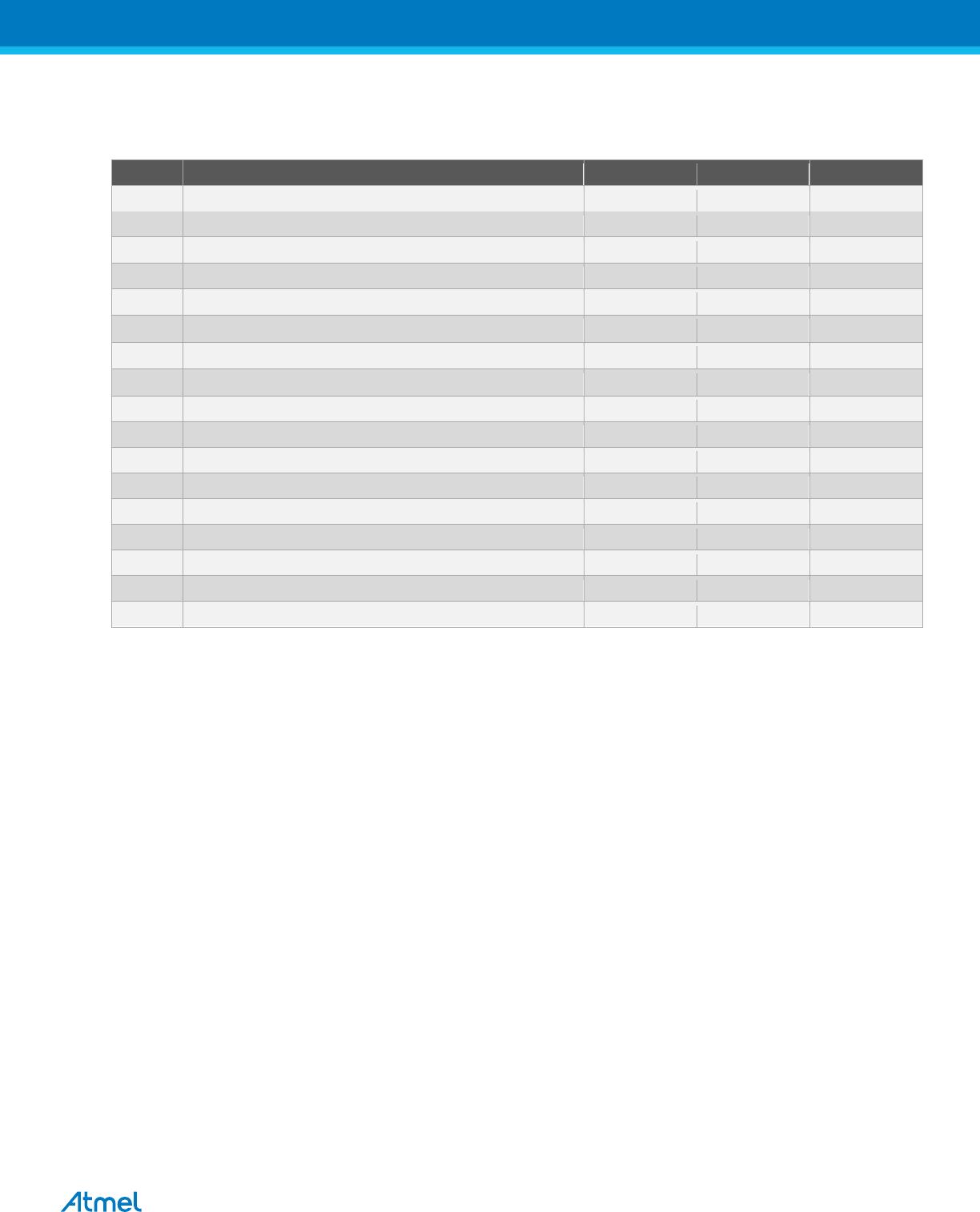
Table 3-1. DC Characteristics
Applicable over recommended operating range from V
CC
= +2.7 to 5.5V, T
AC
= -40°C to +85°C (unless otherwise noted)
Symbol Parameter Test Condition Min Typ Max Units
V
CC
(2)
Supply Voltage 2.7 5.5 V
I
CC
Supply Current (V
CC
= 5.5V) Async Read at 3.57MHz 5 mA
I
CC
Supply Current (V
CC
= 5.5V) Async Write at 3.57MHz 5 mA
I
CC
Supply Current (V
CC
= 5.5V) Synch Read at 1MHz 5 mA
I
CC
Supply Current (V
CC
= 5.5V) Synch Write at 1MHz 5 mA
I
SB
Standby Current (V
CC
= 5.5V) V
IN
= V
CC
or GND 100 mA
V
IL
(1)
SDA/IO Input Low Threshold 0 V
CC
x 0.2 V
V
IL
(1)
SCL/CLK Input Low Threshold 0 V
CC
x 0.2 V
V
IL
(1)
RST Input Low Threshold 0 V
CC
x 0.2 V
V
IH
(1)(2)
SDA/IO Input High Threshold V
CC
x 0.7 V
CC
V
V
IH
(1)(2)
SCL/CLK Input High
Threshold
V
CC
x 0.7 V
CC
V
V
IH
(1)(2)
RST Input High Threshold V
CC
x 0.7 V
CC
V
I
IL
SDA/IO Input Low Current 0 < V
IL
< V
CC
x 0.15 15
µA
I
IL
SCL/CLK Input Low Current 0 < V
IL
< V
CC
x 0.15 15
µA
I
IL
RST Input Low Current 0 < V
IL
< V
CC
x 0.15 50
µA
I
IH
SDA/IO Input High Current V
CC
x 0.7 < V
IH
< V
CC
20
µA
I
IH
SCL/CLK Input High Current V
CC
x 0.7 < V
IH
< V
CC
100
µA
I
IH
RST Input High Current V
CC
x 0.7 < V
IH
< V
CC
150
µA
V
OH
SDA/IO Output High Voltage 20K ohm external pull-up V
CC
x 0.7 V
CC
V
V
OL
SDA/IO Output Low Voltage I
OL
= 1mA 0 V
CC
x 0.15 V
I
OH
SDA/IO Output High Current V
OH
20
µA
Notes: 1. V
IL
min and V
IH
max are reference only and are not tested
2. To prevent latch up conditions from occurring during power up of the AT88SCxxxxC, V
CC
must be turned on
before applying V
IH
. For powering down, V
IH
must be removed before turning V
CC
off
AT88SC0104C [SUMMARY DATASHEET]
Atmel-2021MS-CryptoMem-AT88SC0104C-Datasheet-Summary_122013
5
Table 3-2. AC Characteristics
Applicable over recommended operating range from V
CC
= +2.7 to 5.5V,
T
AC
= -40°C to +85°C, CL = 30pF (unless otherwise noted)
Symbol Parameter Min Max Units
f
CLK
Async Clock Frequency (V
CC
Range: +4.5 - 5.5V) 1 5 MHZ
f
CLK
Async Clock Frequency (V
CC
Range: +2.7 - 3.3V) 1 4 MHZ
f
CLK
Synch Clock Frequency 0 1 MHZ
Clock Duty cycle 40 60 %
t
R
Rise Time - I/O, RST 1
µS
t
F
Fall Time - I/O, RST 1
µS
t
R
Rise Time - CLK 9% x period
µS
t
F
Fall Time - CLK 9% x period
µS
t
AA
Clock Low to Data Out Valid 35 nS
t
HD.STA
Start Hold Time 200 nS
t
SU.STA
Start Set-up Time 200 nS
t
HD.DAT
Data In Hold Time 10 nS
t
SU.DAT
Data In Set-up Time 100 nS
t
SU.STO
Stop Set-up Time 200 nS
t
DH
Data Out Hold Time 20 nS
t
WR
Write Cycle Time (at 25°C) 5 mS
t
WR
Write Cycle Time (-40° to +85°C) 7 mS
4. Device Operation for Synchronous Protocols
Clock and Data Transitions:
The SDA pin is normally pulled high with an external device. Data on the SDA pin may change only during SCL low time
periods (see Figure 4-3 on page 7). Data changes during SCL high periods will indicate a start or stop condition as defined
below.
Start Condition:
A high-to-low transition of SDA with SCL high is a start condition which must precede any other command (see Figure 4-4 on
page 7).
Stop Condition:
A low-to-high transition of SDA with SCL high is a stop condition. After a read sequence, the stop command will place the
EEPROM in a standby power mode (see Figure 4-4 on page 7).
Acknowledge:
All addresses and data words are serially transmitted to and from the EEPROM in 8-bit words. The EEPROM sends a zero to
acknowledge that it has received each word. This happens during the ninth clock cycle (see Figure 4-5 on page 7).
Memory Reset:
After an interruption in protocol, power loss or system reset, any 2-wire part can be reset by following these steps:
1. Clock up to nine cycles
2. Look for SDA high in each cycle while SCL is high
3. Create a start condition
AT88SC0104C [SUMMARY DATASHEET]
Atmel-2021MS-CryptoMem-AT88SC0104C-Datasheet-Summary_122013
6
Figure 4-1. Bus Timing for 2-wire Communications
SCL: Serial Clock, SDA Serial Data I/O
Figure 4-2. Write Cycle Timing
SCL: Serial Clock, SDA Serial Data I/O
Note: The write cycle time t
WR
is the time from a valid stop condition of a write sequence to the end of the internal
clear/write cycle
t
wr
(1)
STOP
CONDITION
START
CONDITION
WORDn
ACK
8th BIT
SCL
SDA

AT88SC0104C-MJ

Mfr. #:
Manufacturer:
Microchip Technology / Atmel
Description:
EEPROM CRYPTO Memory 1Kbit, 4zones
Lifecycle:
New from this manufacturer.
Delivery:
DHL FedEx Ups TNT EMS
Payment:
T/T Paypal Visa MoneyGram Western Union