7
SAM9N12/SAM9CN11/SAM9CN12 [SUMMARY DATASHEET]
11063HS–ATARM–27-Sep-13
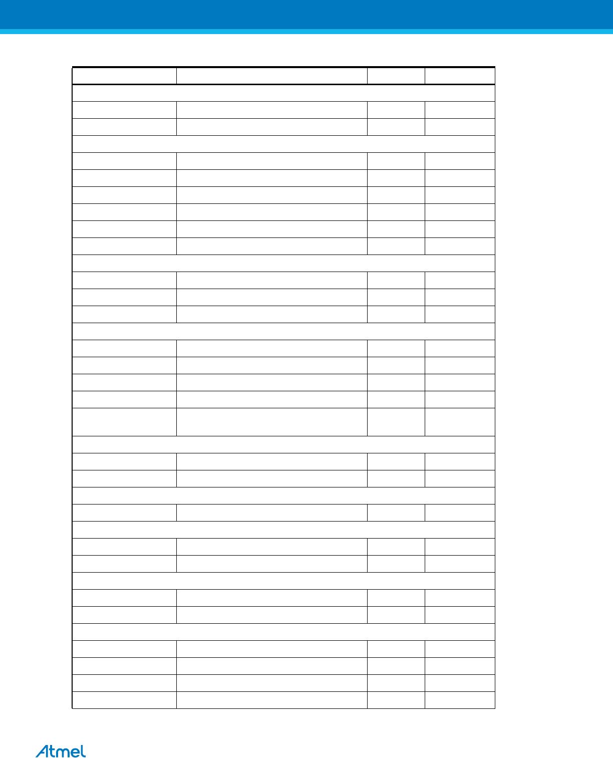
Universal Asynchronous Receiver Transmitter - UARTx
UTXDx UARTx Transmit Data Output
URXDx UARTx Receive Data Input
Synchronous Serial Controller - SSC
TD SSC Transmit Data Output
RD SSC Receive Data Input
TK SSC Transmit Clock I/O
RK SSC Receive Clock I/O
TF SSC Transmit Frame Sync I/O
RF SSC Receive Frame Sync I/O
Timer Counter - TCx x=0..5
TCLKx TC Channel x External Clock Input Input
TIOAx TC Channel x I/O Line A I/O
TIOBx TC Channel x I/O Line B I/O
Serial Peripheral Interface - SPIx
SPIx_MISO Master In Slave Out I/O
SPIx_MOSI Master Out Slave In I/O
SPIx_SPCK SPI Serial Clock I/O
SPIx_NPCS0 SPI Peripheral Chip Select 0 I/O Low
SPIx_NPCS1-
SPIx_NPCS3
SPI Peripheral Chip Select Output Low
Two-wire Interface -TWIx
TWDx Two-wire Serial Data I/O
TWCKx Two-wire Serial Clock I/O
Pulse Width Modulation Controller- PWM
PWM0 - PWM3 Pulse Width Modulation Output Output
USB Device Full Speed Port - UDP
DDP USB Device Data + Analog
DDM USB Device Data - Analog
USB Host Full Speed Port - UHP
HDP USB Host Data + Analog
HDM USB Host Data - Analog
LCD Controller - LCDC
LCDDAT 0-23 LCD Data Bus Output
LCDVSYNC LCD Vertical Synchronization Output
LCDHSYNC LCD Horizontal Synchronization Output
LCDPCK LCD Pixel Clock Output
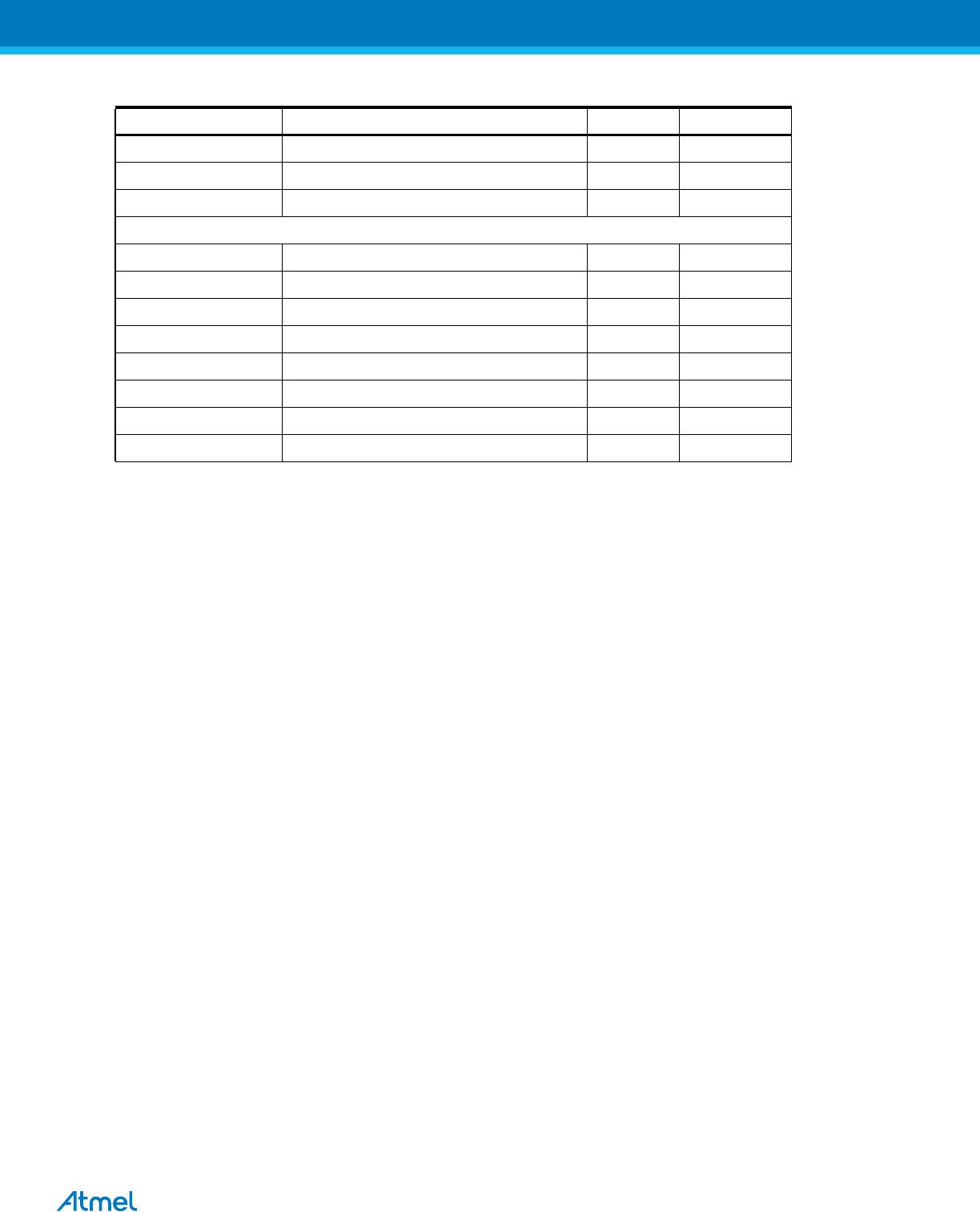
Table 3-1. Signal Description List (Continued)
Signal Name Function Type Active Level