DS058 (v1.9) April 3, 2007 www.xilinx.com 1
Product Specification
© 2006 Xilinx, Inc. All rights reserved. All Xilinx trademarks, registered trademarks, patents, and disclaimers are as listed at http://www.xilinx.com/legal.htm.
All other trademarks and registered trademarks are the property of their respective owners. All specifications are subject to change without notice.
Features
• 5 ns pin-to-pin logic delays
• System frequency up to 178 MHz
• 36 macrocells with 800 usable gates
• Available in small footprint packages
- 44-pin PLCC (34 user I/O pins)
- 44-pin VQFP (34 user I/O pins)
- 48-pin CSP (36 user I/O pins)
- 64-pin VQFP (36 user I/O pins)
- Pb-free available for all packages
• Optimized for high-performance 3.3V systems
- Low power operation
- 5V tolerant I/O pins accept 5 V, 3.3V, and 2.5V
signals
- 3.3V or 2.5V output capability
- Advanced 0.35 micron feature size CMOS
Fast FLASH™ technology
• Advanced system features
- In-system programmable
- Superior pin-locking and routability with
Fast CONNECT™ II switch matrix
- Extra wide 54-input Function Blocks
- Up to 90 product-terms per macrocell with
individual product-term allocation
- Local clock inversion with three global and one
product-term clocks
- Individual output enable per output pin
- Input hysteresis on all user and boundary-scan pin
inputs
- Bus-hold circuitry on all user pin inputs
- Full IEEE Standard 1149.1 boundary-scan (JTAG)
• Fast concurrent programming
• Slew rate control on individual outputs
• Enhanced data security features
• Excellent quality and reliability
- Endurance exceeding 10,000 program/erase
cycles
- 20 year data retention
- ESD protection exceeding 2,000V
• Pin-compatible with 5V-core XC9536 device in the
44-pin PLCC package and the 48-pin CSP package
WARNING: Programming temperature range of
T
A
= 0° C to +70° C
Description
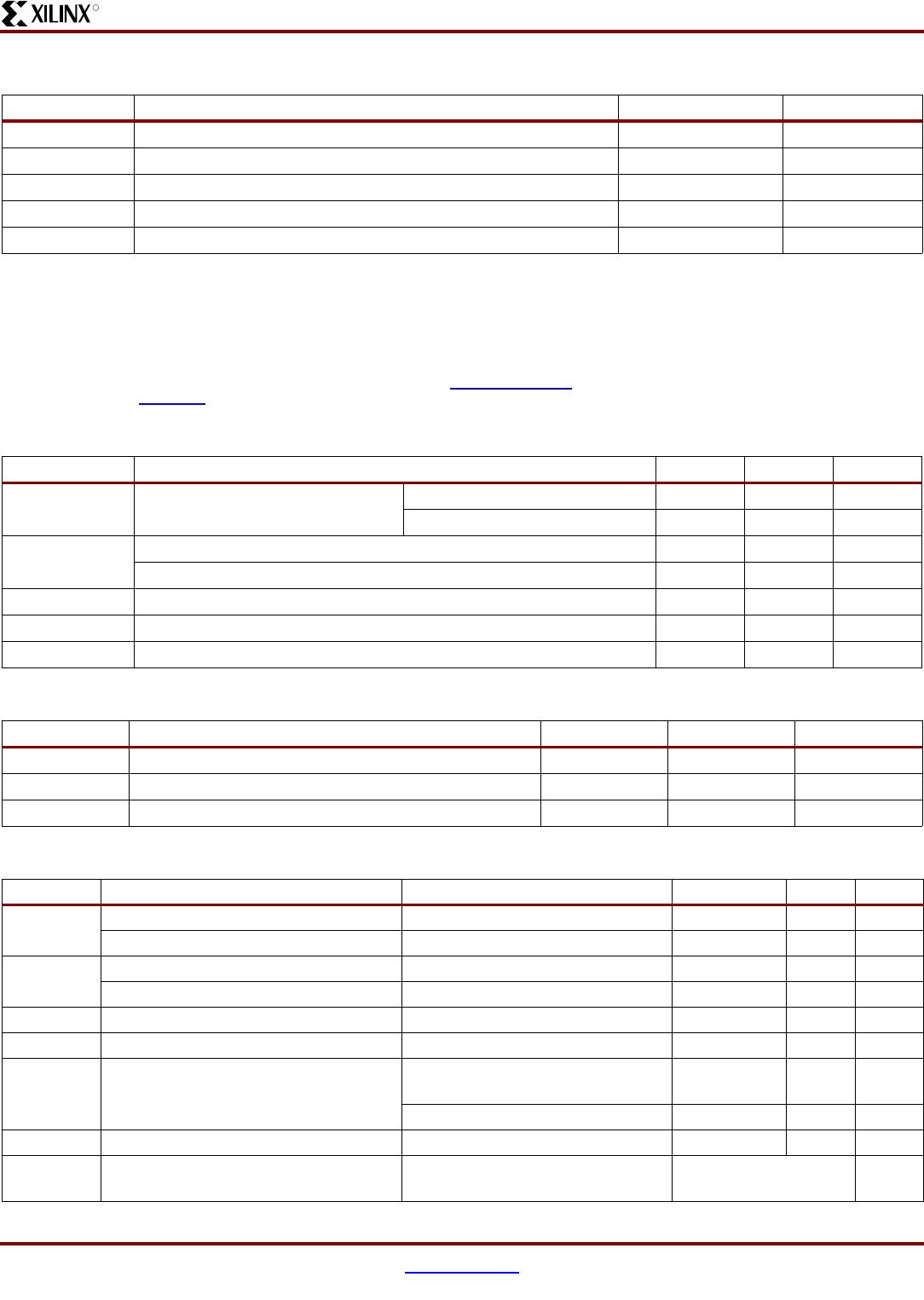
The XC9536XL is a 3.3V CPLD targeted for high-perfor-
mance, low-voltage applications in leading-edge communi-
cations and computing systems. It is comprised of two
54V18 Function Blocks, providing 800 usable gates with
propagation delays of 5 ns. See Figure 2 for architecture
overview.
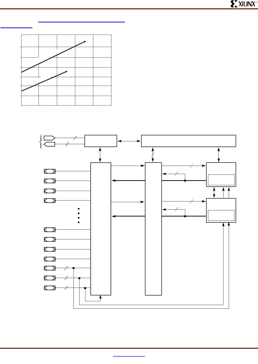
Power Estimation
Power dissipation in CPLDs can vary substantially depend-
ing on the system frequency, design application and output
loading. To help reduce power dissipation, each macrocell
in a XC9500XL device may be configured for low-power
mode (from the default high-performance mode). In addi-
tion, unused product-terms and macrocells are automati-
cally deactivated by the software to further conserve power.
For a general estimate of I
CC
, the following equation may be
used:
I
CC
(mA) = MC
HS
(0.175*PT
HS
+ 0.345) + MC
LP
(0.052*PT
LP
+ 0.272) + 0.04 * MC
TOG
(MC
HS
+MC
LP
)* f
where:
MC
HS
= # macrocells in high-speed configuration
PT
HS
= average number of high-speed product terms
per macrocell
MC
LP
= # macrocells in low power configuration
PT
LP
= average number of low power product terms per
macrocell
f = maximum clock frequency
MCTOG = average % of flip-flops toggling per clock
(~12%)
This calculation was derived from laboratory measurements
of an XC9500XL part filled with 16-bit counters and allowing
a single output (the LSB) to be enabled. The actual I
CC
value varies with the design application and should be veri-
fied during normal system operation. Figure 1 shows the
above estimation in a graphical form. For a more detailed
discussion of power consumption in this device, see Xilinx
0
XC9536XL High Performance
CPLD
DS058 (v1.9) April 3, 2007
00
Product Specification
R