VS-VSKL71/10

VS-VSKT71.., VS-VSKH71.., VS-VSKL71.., VS-VSKN71.. Series
www.vishay.com
Vishay Semiconductors
Revision: 21-Mar-14
4
Document Number: 94631
For technical questions within your region: DiodesAmericas@vishay.com
, DiodesAsia@vishay.com, DiodesEurope@vishay.com
THIS DOCUMENT IS SUBJECT TO CHANGE WITHOUT NOTICE. THE PRODUCTS DESCRIBED HEREIN AND THIS DOCUMENT
ARE SUBJECT TO SPECIFIC DISCLAIMERS, SET FORTH AT www.vishay.com/doc?91000
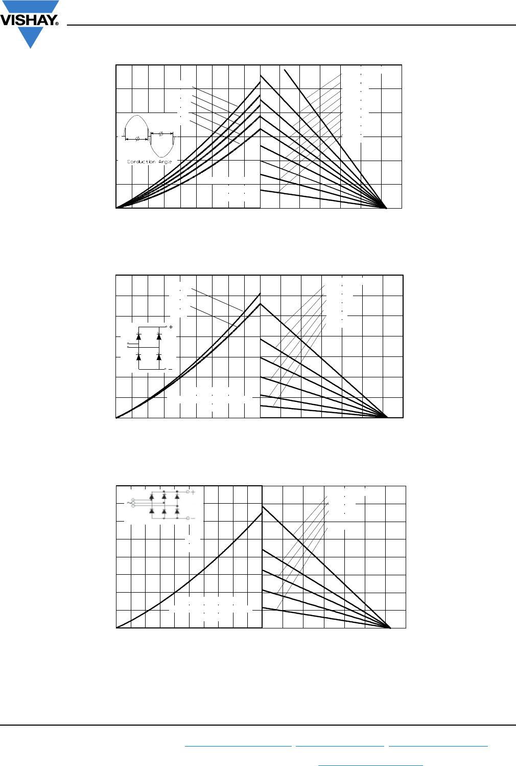
Fig. 1 - Current Ratings Characteristics
Fig. 2 - Current Ratings Characteristics
Fig. 3 - On-State Power Loss Characteristics
Fig. 4 - On-State Power Loss Characteristics
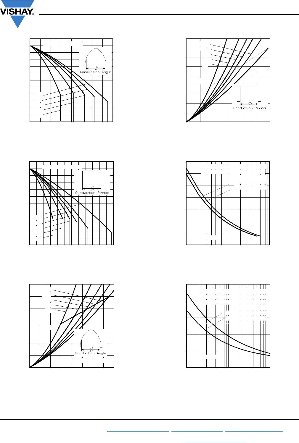
Fig. 5 - Maximum Non-Repetitive Surge Current
Fig. 6 - Maximum Non-Repetitive Surge Current
Average on-state current (A)
Maximum allowable case temperature (°C)
0 1020304050607080
70
80
90
100
110
120
130
180°
120°
90°
60°
30°
RthJC (DC) = 0.29°C/W
0 20406080100120
70
80
90
100
110
120
130
180°
120°
90°
60°
30°
DC
RthJC (DC) = 0.29°C/W
Average on-state current (A)
Maximum allowable case temperature (°C)
Average on-state current (A)
Maximum average on-state power loss (W)
0 1020304050607080
0
20
40
60
80
100
120
140
180°
120°
90°
60°
30°
RMS limit
Per leg, Tj = 125°C
Average on-state current (A)
Maximum average on-state power loss (W)
020406080100120
0
20
40
60
80
100
120
140
160
180
180°
120°
90°
60°
30°
RMS limit
DC
Per leg, Tj = 125°C
Peak half sine wave on-state current (A)
Number of equal amplitude half cycle current pulses (N)
110100
500
600
700
800
900
1000
1100
1200
At any rated load condition and with
rated Vrrm applied following surge
Initial Tj = Tj max
@ 60 Hz 0.0083 s
@ 50 Hz 0.0100s
Per leg
Peak half sine wave on-state current (A)
Pulse train duration (s)
0.01 0.1 1
400
600
800
1000
1200
1400
Maximum Non-repetitive Surge Current
Versus Pulse Train Duration. Control
of conduction may not be maintained.
Initial Tj = 125°C
No Voltage Reapplied
Rated Vrrm reapplied
Per leg
VS-VSKT71.., VS-VSKH71.., VS-VSKL71.., VS-VSKN71.. Series
www.vishay.com
Vishay Semiconductors
Revision: 21-Mar-14
5
Document Number: 94631
For technical questions within your region: DiodesAmericas@vishay.com
, DiodesAsia@vishay.com, DiodesEurope@vishay.com
THIS DOCUMENT IS SUBJECT TO CHANGE WITHOUT NOTICE. THE PRODUCTS DESCRIBED HEREIN AND THIS DOCUMENT
ARE SUBJECT TO SPECIFIC DISCLAIMERS, SET FORTH AT www.vishay.com/doc?91000
Fig. 7 - On-State Power Loss Characteristics
Fig. 8 - On-State Power Loss Characteristics
Fig. 9 - On-State Power Loss Characteristics
Total RMS output current (A)
Maximum total on-state power loss (W)
Maximum allowable ambient temperature (°C)
0 20 40 60 80 100 120 140
RthSA = 0.1 °C/W
0.2 °C/W
0.3 °C/W
0.4 °C/W
0.5 °C/W
0.7 °C/W
1 °C/W
1.5 °C/W
3 °C/W
0 20 40 60 80 100 120 140 160 180
0
50
100
150
200
250
300
180°
120°
90°
60°
30°
VSK.71 Series
Per module
Tj = 125°C
Total output current (A)
Maximum total power loss (W)
0 20 40 60 80 100 120 140
RthSA = 0.1 °C/W
0.2 °C/W
0.3 °C/W
0.5 °C/W
1 °C/W
2 °C/W
Maximum allowable ambient temperature (°C)
0 20 40 60 80 100 120 140 160 180
0
100
200
300
400
500
600
700
180°
(sine)
180°
(rect)
2 x VSK.71 Series
single phase bridge connected
Tj = 125°C
Total output current (A)
Maximum allowable ambient temperature (°C)
Maximum total power loss (W)
0 20 40 60 80 100 120 140
RthSA = 0.1 °C/W
0.2 °C/W
0.3 °C/W
0.5 °C/W
1 °C/W
04080120160200
0
100
200
300
400
500
600
700
800
120°
(rect)
3 x VSK.71 Series
three phase bridge connected
Tj = 125°C
VS-VSKT71.., VS-VSKH71.., VS-VSKL71.., VS-VSKN71.. Series
www.vishay.com
Vishay Semiconductors
Revision: 21-Mar-14
6
Document Number: 94631
For technical questions within your region: DiodesAmericas@vishay.com
, DiodesAsia@vishay.com, DiodesEurope@vishay.com
THIS DOCUMENT IS SUBJECT TO CHANGE WITHOUT NOTICE. THE PRODUCTS DESCRIBED HEREIN AND THIS DOCUMENT
ARE SUBJECT TO SPECIFIC DISCLAIMERS, SET FORTH AT www.vishay.com/doc?91000
Fig. 10 - On-State Voltage Drop Characteristics
Fig. 11 - Thermal Impedance Z
thJC
Characteristics
Fig. 12 - Gate Characteristics
Instantaneous on-state voltage (V)
Instantaneous on-state current (A)
0.5 1.0 1.5 2.0 2.5 3.0 3.5
1
10
100
1000
Tj = 25°C
Tj = 125°C
Per leg
Square wave pulse duration (s)
Transient thermal impedance Z
thJC
(°C/W)
0.001 0.01 0.1 1 10
0.01
0.1
1
Steady state value
RthJC = 0.29 °C/W
(DC operation)
Per leg
0.1
1
10
100
0.001 0.01 0.1 1 10 100 1000
(b)
(a)
Rectangular gate pulse
(4) (3) (2) (1)
TJ = - 4 0 ° C
TJ = 2 5 ° C
TJ = 1 2 5 ° C
a)Recommended load line for
b)Recommended load line for
VGD
IGD
Fr e q u e n c y Li m i t e d b y PG ( A V )
(1) PGM = 200 W, tp = 300 µs
(2) PGM = 60 W, tp = 1 ms
(3) PGM = 30 W, tp = 2 ms
(4) PGM = 12 W, tp = 5 ms
<= 30% ra t ed d i/ d t : 15 V, 40 o h ms
tr = 1 µs, tp >= 6 µs
rated di/dt: 20 V, 20 ohms
tr = 0.5 µs, tp >= 6 µs
IRK.71../ .91.. Series
Instantaneous gate voltage (V)
Instantaneous gate current (A)
VSK.71

VS-VSKL71/10

Mfr. #:
Manufacturer:
Vishay Semiconductors
Description:
SCR Modules 1000 Volt 75 Amp 1360 Amp IFSM
Lifecycle:
New from this manufacturer.
Delivery:
DHL FedEx Ups TNT EMS
Payment:
T/T Paypal Visa MoneyGram Western Union