DS112 (v3.1) August 30, 2010 www.xilinx.com
Product Specification 1
© Copyright 2004–2010 Xilinx, Inc. XILINX, the Xilinx logo, Virtex, Spartan, ISE, and other designated brands included herein are trademarks of Xilinx in the United States and
other countries. The PowerPC name and logo are registered trademarks of IBM Corp. and used under license. All other trademarks are the property of their respective owners.
`
General Description
Combining Advanced Silicon Modular Block (ASMBL™) architecture with a wide variety of flexible features, the Virtex®-4
family from Xilinx greatly enhances programmable logic design capabilities, making it a powerful alternative to ASIC
technology. Virtex-4 FPGAs comprise three platform families—LX, FX, and SX—offering multiple feature choices and
combinations to address all complex applications. The wide array of Virtex-4 FPGA hard-IP core blocks includes the
PowerPC® processors (with a new APU interface), tri-mode Ethernet MACs, 622 Mb/s to 6.5 Gb/s serial transceivers,
dedicated DSP slices, high-speed clock management circuitry, and source-synchronous interface blocks. The basic Virtex-4
FPGA building blocks are enhancements of those found in the popular Virtex, Virtex-E, Virtex-II, Virtex-II Pro, and
Virtex-II Pro X product families, so previous-generation designs are upward compatible. Virtex-4 devices are produced on a
state-of-the-art 90 nm copper process using 300 mm (12-inch) wafer technology.
Summary of Virtex-4 Family Features
• Three Families — LX/SX/FX
- Virtex-4 LX: High-performance logic applications solution
- Virtex-4 SX: High-performance solution for digital signal
processing (DSP) applications
- Virtex-4 FX: High-performance, full-featured solution for
embedded platform applications
• Xesium™ Clock Technology
- Digital clock manager (DCM) blocks
- Additional phase-matched clock dividers (PMCD)
- Differential global clocks
• XtremeDSP™ Slice
- 18 x 18, two’s complement, signed Multiplier
- Optional pipeline stages
- Built-in Accumulator (48-bit) and Adder/Subtracter
• Smart RAM Memory Hierarchy
- Distributed RAM
- Dual-port 18-Kbit RAM blocks
· Optional pipeline stages
· Optional programmable FIFO logic automatically
remaps RAM signals as FIFO signals
- High-speed memory interface supports DDR and DDR-2
SDRAM, QDR-II, and RLDRAM-II.
• SelectIO™ Technology
- 1.5V to 3.3V I/O operation
- Built-in ChipSync™ source-synchronous technology
- Digitally controlled impedance (DCI) active termination
- Fine grained I/O banking (configuration in one bank)
• Flexible Logic Resources
• Secure Chip AES Bitstream Encryption
• 90 nm Copper CMOS Process
• 1.2V Core Voltage
• Flip-Chip Packaging including Pb-Free Package
Choices
• RocketIO™ 622 Mb/s to 6.5 Gb/s Multi-Gigabit
Transceiver (MGT) [FX only]
• IBM PowerPC RISC Processor Core [FX only]
- PowerPC 405 (PPC405) Core
- Auxiliary Processor Unit Interface (User Coprocessor)
• Multiple Tri-Mode Ethernet MACs [FX only]
0
Virtex-4 Family Overview
DS112 (v3.1) August 30, 2010
00
Product Specification
R
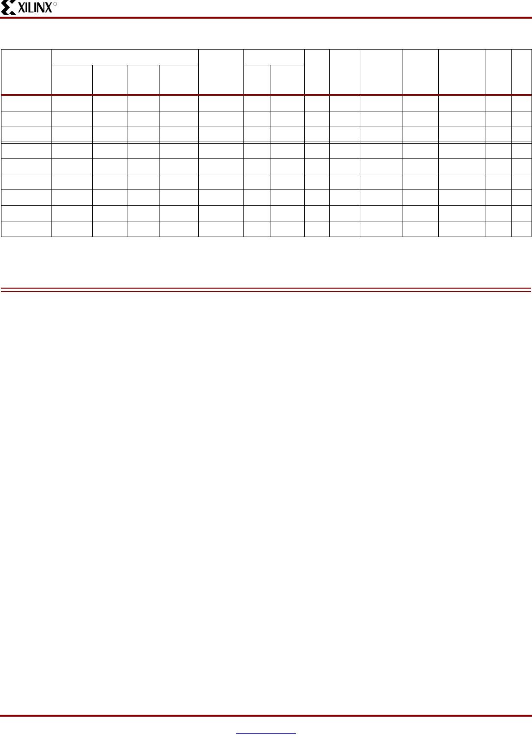
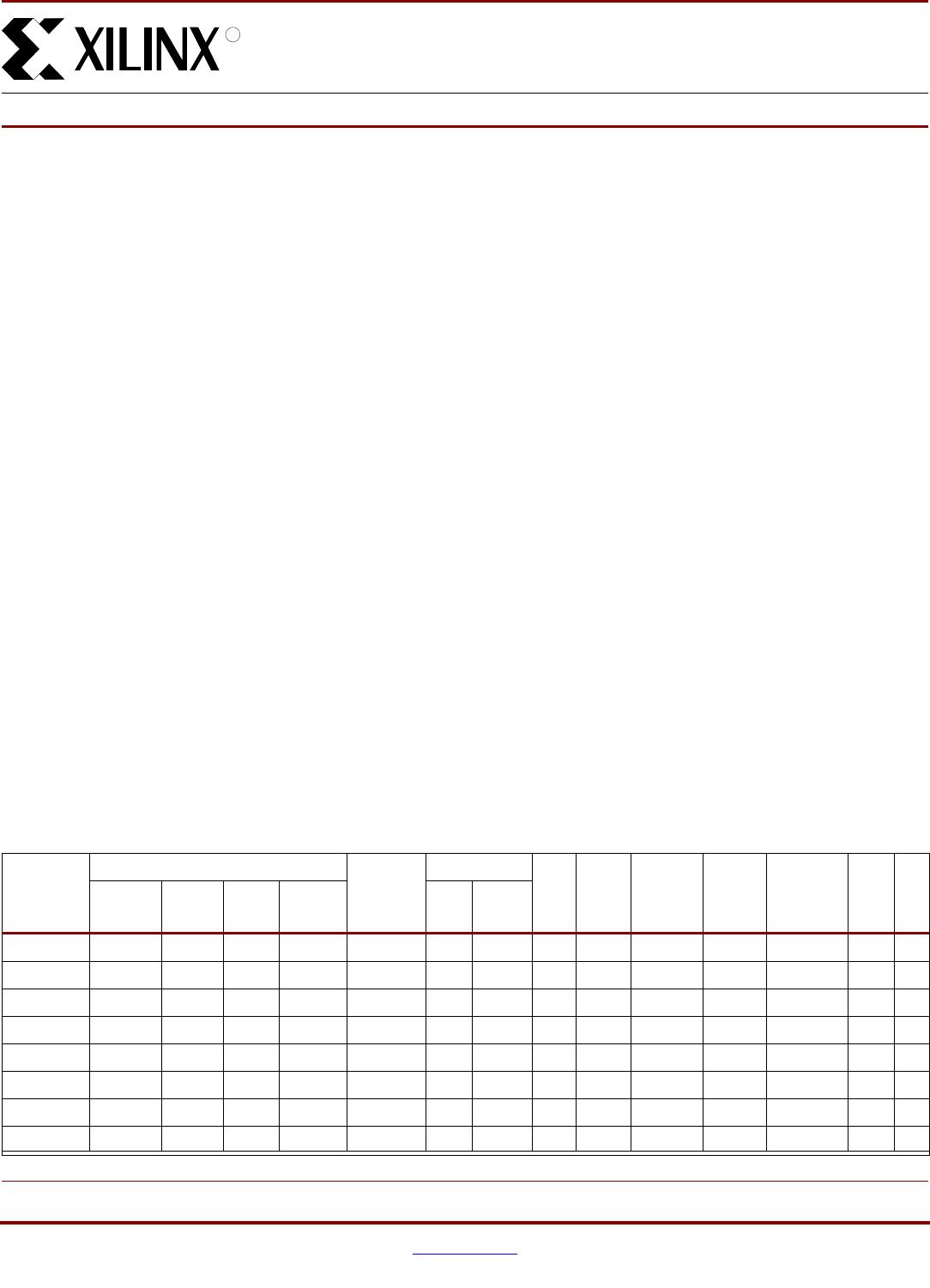
Table 1: Virtex-4 FPGA Family Members
Device
Configurable Logic Blocks (CLBs)
(1)
XtremeDSP
Slices
(2)
Block RAM
DCMs PMCDs
PowerPC
Processor
Blocks
Ethernet
MACs
RocketIO
Transceiver
Blocks
Total
I/O
Banks
Max
User
I/O
Array
(3)
Row x Col
Logic
Cells Slices
Max
Distributed
RAM (Kb)
18 Kb
Blocks
Max
Block
RAM (Kb)
XC4VLX15 64 x 24 13,824 6,144 96
32
48 864 4 0 N/A N/A N/A 9 320
XC4VLX25 96 x 28 24,192 10,752 168
48
72 1,296 8 4 N/A N/A N/A 11 448
XC4VLX40 128 x 36 41,472 18,432 288
64
96 1,728 8 4 N/A N/A N/A 13 640
XC4VLX60 128 x 52 59,904 26,624 416
64
160 2,880 8 4 N/A N/A N/A 13 640
XC4VLX80 160 x 56 80,640 35,840 560
80
200 3,600 12 8 N/A N/A N/A 15 768
XC4VLX100 192 x 64 110,592 49,152 768
96
240 4,320 12 8 N/A N/A N/A 17 960
XC4VLX160 192 x 88 152,064 67,584 1056
96
288 5,184 12 8 N/A N/A N/A 17 960
XC4VLX200 192 x 116 200,448 89,088 1392
96
336 6,048 12 8 N/A N/A N/A 17 960