TECHNICAL DATA SHEET
6 Lake Street, Lawrence, MA 01841
1-800-446-1158 / (978) 620-2600 / Fax: (978) 689-0803
Website: http: //www.microsemi.com
T4-LDS-0060 Rev. 2 (100247) Page 4 of 6
NOTES:
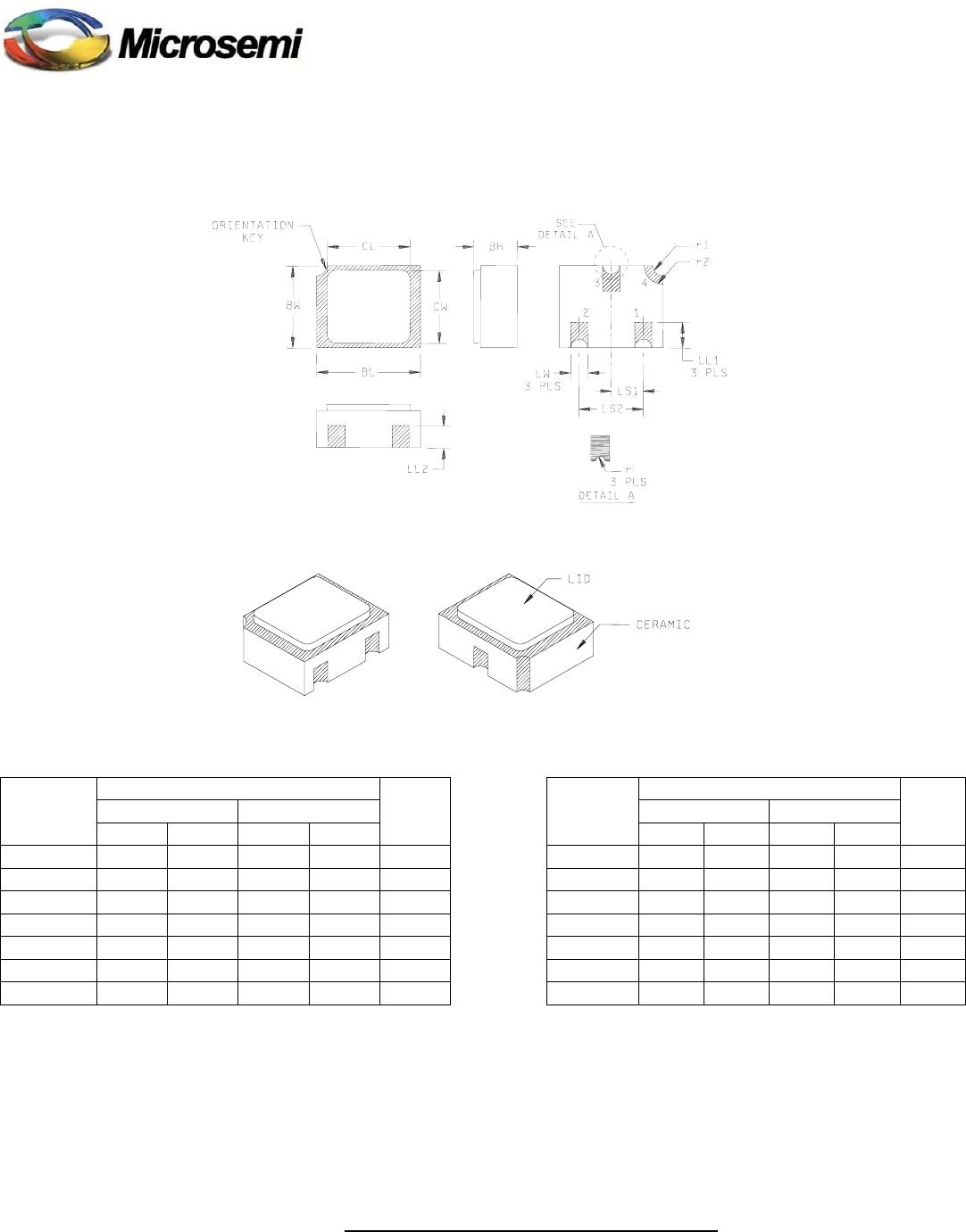
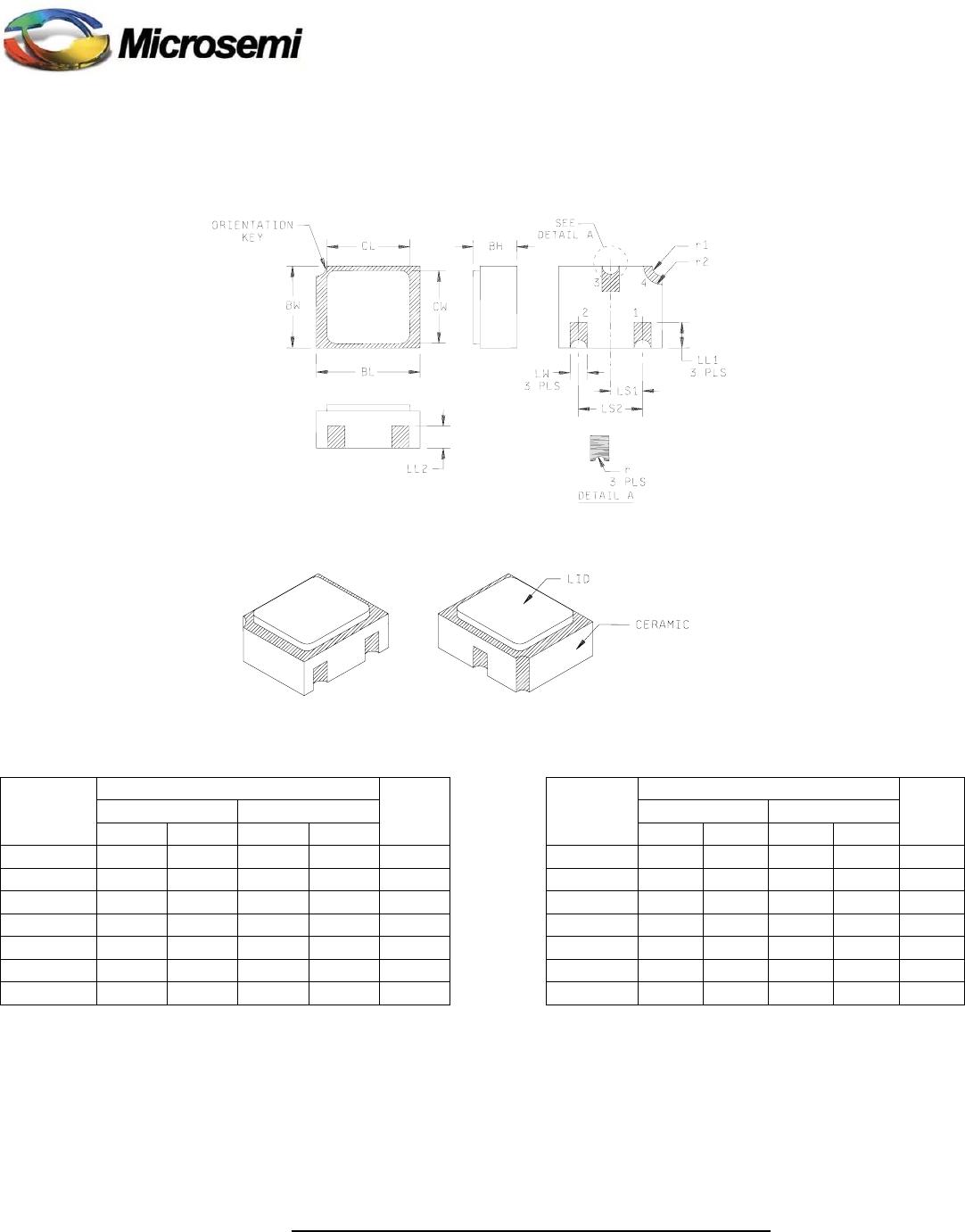
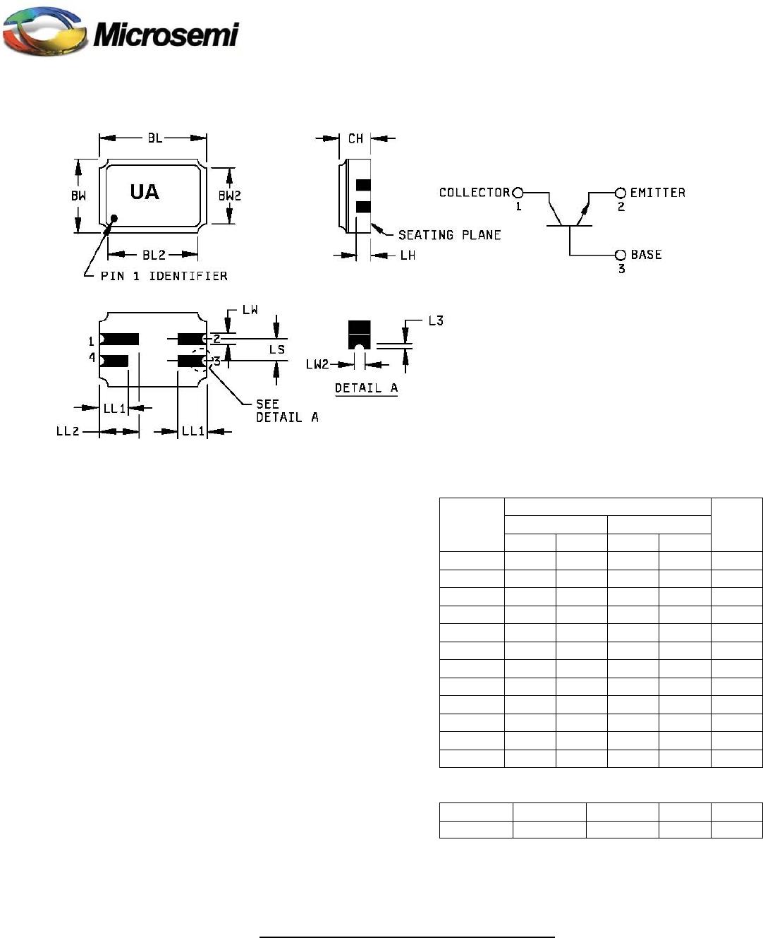
Dimensions
1. Dimensions are in inches.
Symbol
Inches Millimeters
Note
2. Millimeters are given for general information only.
Min Max Min Max
3. Dimension CH controls the overall package thickness. When a BL .215 .225 5.46 5.71
window lid is used, dimension CH must increase by a minimum of BL2
.225 5.71
.010 inch (0.254 mm) and a maximum of .040 inch (1.020 mm). BW .145 .155 3.68 3.93
4. The corner shape (square, notch, radius) may vary at the BW2
.155 3.93
manufacturer's option, from that shown on the drawing. CH .061 .075 1.55 1.90 3
5. Dimensions LW2 minimum and L3 minimum and the appropriate L3
.003 .007 0.08 0.18 5
castellation length define an unobstructed three-dimensional space LH .029 .042 0.74 1.07
traversing all of the ceramic layers in which a castellation was LL1
.032 .048 0.81 1.22
designed. (Castellations are required on the bottom two layers, LL2
.072 .088 1.83 2.23
optional on the top ceramic layer.) Dimension LW2 maximum and LS .045 .055 1.14 1.39
L3 maximum define the maximum width and depth of the LW .022 .028 0.56 0.71
castellation at any point on its surface. Measurement of these LW2
.006 .022 0.15 0.56 5
dimensions may be made prior to solder dipping.
6. The co-planarity deviation of all terminal contact points, as defined
by the device seating plane, shall not exceed .006 inch (0.15mm) for Pin no. 1 2 3 4
solder dipped leadless chip carriers. Transistor Collector Emitter Base N/C
7. In accordance with ASME Y14.5M, diameters are equivalent to φx
symbology.
FIGURE 2. Physical dimensions, surface mount (UA version).