PDF: 09005aef817f1b8c/Source: 09005aef818112f1 Micron Technology, Inc., reserves the right to change products or specifications without notice.
512Mb Mobile SDRAM_TwinDie_x32.fm - Rev. C 6/05 EN
2 ©2004 Micron Technology, Inc. All rights reserved.
512Mb : x32 TwinDie Mobile SDRAM Addendum
General Description
General Description
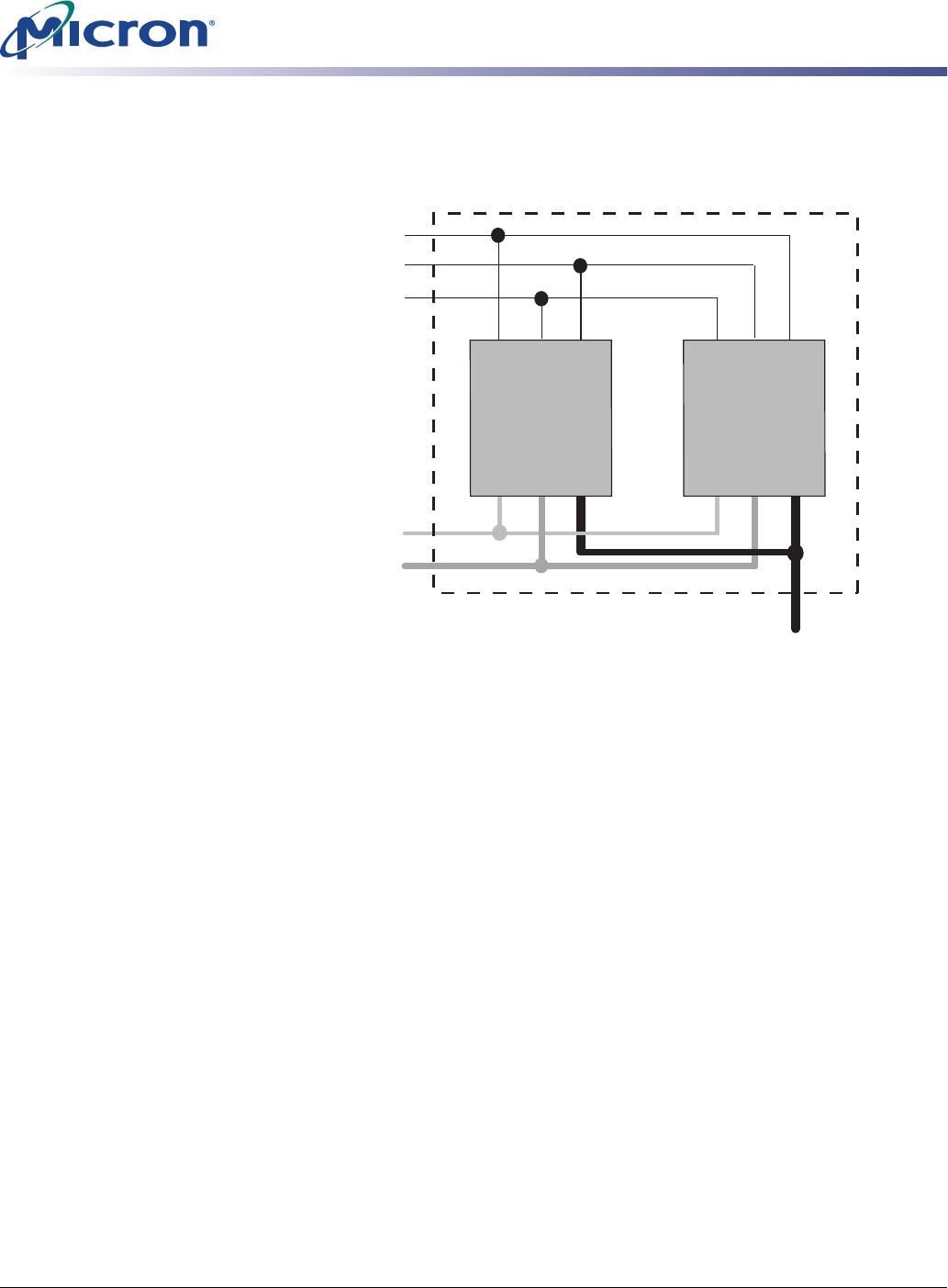
The 512Mb SDRAM is a high-speed CMOS, dynamic random-access memory containing
536,870,912 bits. It is internally configured by stacking two 256Mb, 8 Meg x 32 devices.
Each of these 256Mb devices is configured as a quad bank DRAM with a synchronous
interface. They are organized with 32 DQs with 4 banks of 67,108,864 bits, comprising of
8,192 rows by 512 columns by 32 bits wide.
Read and write accesses to the SDRAM are burst oriented; accesses start at a selected
location and continue for a programmed number of locations in a programmed
sequence. Accesses begin with the registration of an ACTIVE command, which is then
followed by a READ or WRITE command. The address bits registered coincident with the
ACTIVE command are used to select the bank and row to be accessed (BA0, BA1 select
the bank; A0-A12 select the row). The address bits registered coincident with the READ
or WRITE command are used to select the starting column location for the burst access.
The SDRAM provides for programmable READ or WRITE burst lengths of 1, 2, 4, or 8
locations, or the full page, with a burst terminate option. An auto precharge function
may be enabled to provide a self-timed row precharge that is initiated at the end of the
burst sequence.
The 512Mb SDRAM uses an internal pipelined architecture to achieve high-speed opera-
tion. This architecture is compatible with the 2n rule of prefetch architectures, but it also
allows the column address to be changed on every clock cycle to achieve a high-speed,
fully random access. Precharging one bank while accessing one of the other three banks
will hide the precharge cycles and provide seamless, high-speed, random-access opera-
tion.
The 512Mb SDRAM is designed to operate in 3.3V, 2.5V, and 1.8V memory systems. An
auto refresh mode is provided, along with a power-saving, power-down mode. All inputs
and outputs are LVTTL-compatible.
SDRAMs offer substantial advances in DRAM operating performance, including the abil-
ity to synchronously burst data at a high data rate with automatic column-address gen-
eration, the ability to interleave between internal banks to hide precharge time, and the
capability to randomly change column addresses on each clock cycle during a burst
access.
Prior to normal operation, the SDRAM must be initialized. The following sections pro-
vide detailed information covering die intitialization, register definition, command
descriptions, and device operation on a per die basis unless otherwise noted.
This addendum documents any variances for the 512Mb: x32 Mobile SDRAM from the
256Mb: x32 Mobile SDRAM specification. Please refer to the 256Mb: x32 Mobile SDRAM
data sheet on Micron’s Web site for additional details on the part functionality.
Commands
AUTO REFRESH
AUTO REFRESH is used during normal operation of the SDRAM and is analogous to
CAS#-BEFORE-RAS# (CBR) REFRESH in conventional DRAMs. This command is non-
persistent, so it must be issued each time a refresh is required. All active banks must be
PRECHARGED prior to issuing a AUTO REFRESH command. The AUTO REFRESH com-
mand should not be issued until the minimum
t
RP has been met after the PRECHARGE
command as shown in the operations section.
The addressing is generated by the internal refresh controller. This makes the address
bits “Don’t Care” during an AUTO REFRESH command. The 512Mb TwinDie™ Mobile
SDRAM requires 8,192 AUTO REFRESH cycles every 64ms (
t
REF). Providing a distributed