MT48H16M32L2F5-10 TR

PDF: 09005aef817f1b8c/Source: 09005aef818112f1 Micron Technology, Inc., reserves the right to change products or specifications without notice.
512Mb Mobile SDRAM_TwinDie_x32.fm - Rev. C 6/05 EN
4 ©2004 Micron Technology, Inc. All rights reserved.
512Mb : x32 TwinDie Mobile SDRAM Addendum
Ball Assignment
Ball Assignment
Figure 2: 90-Ball FBGA Assignment
1234 67895
DQ26
DQ28
V
SSQ
V
SSQ
V
DDQ
V
SS
A4
A7
CLK
DQM1
V
DDQ
V
SSQ
V
SSQ
DQ11
DQ13
DQ24
V
DDQ
DQ27
DQ29
DQ31
DQM3
A5
A8
CKE
NC
DQ8
DQ10
DQ12
V
DDQ
DQ15
V
SS
VSSQ
DQ25
DQ30
NC
A3
A6
A12
A9
NC
V
SS
DQ9
DQ14
V
SSQ
V
SS
VDD
VDDQ
DQ22
DQ17
NC
A2
A10
NC
BA0
CAS#
V
DD
DQ6
DQ1
V
DDQ
V
DD
DQ21
DQ19
V
DDQ
V
DDQ
V
SSQ
V
DD
A1
A11
RAS#
DQM0
V
SSQ
V
DDQ
V
DDQ
DQ4
DQ2
DQ23
V
SSQ
DQ20
DQ18
DQ16
DQM2
A0
BA1
CS#
WE#
DQ7
DQ5
DQ3
V
SSQ
DQ0
A
B
C
D
E
F
G
H
J
K
L
M
N
P
R
Ball and Array
PDF: 09005aef817f1b8c/Source: 09005aef818112f1 Micron Technology, Inc., reserves the right to change products or specifications without notice.
512Mb Mobile SDRAM_TwinDie_x32.fm - Rev. C 6/05 EN
5 ©2004 Micron Technology, Inc. All rights reserved.
512Mb : x32 TwinDie Mobile SDRAM Addendum
Electrical Specifications
Table 3: DC Electrical Characteristics and Operating Conditions (LC version)
VDD/VDDQ = +3.3V ±0.3V
Notes: 1, 5, 6; please refer to the 256Mb: x32 Mobile SDRAM data sheet for all notes.
Parameter/Condition Symbol MIN MAX Units Notes
Supply Voltage
VDD/VDDQ 33.6V
Input High Voltage: Logic 1; All inputs
VIH 0.8 x VDDQ VDD + 0.3 V22
Input Low Voltage: Logic 0; All inputs
VIL -0.3 0.3 V 22
Input Leakage Current:
Any input 0V V
IN VDD
(All other balls not under test = 0V)
II -5 5 µA
Output Leakage Current: DQs are disabled; 0V V
OUT
VDDQ
IOZ -5 5 µA
Output Levels:
Output High Voltage (IOUT = -4mA)
V
OH VDDQ - 0.2 V
Output Low Voltage (IOUT = 4mA)
V
OL –0.2V
Table 4: DC Electrical Characteristics and Operating Conditions (V version)
VDD = +2.5V ±0.2V VDDQ = +2.5V ±0.2V or VDDQ = +1.8V ±0.15V
Notes: 1, 5, 6; please refer to the 256Mb: x32 Mobile SDRAM data sheet for all notes.
Parameter/Condition Symbol MIN MAX Units Notes
Supply Voltage
VDD/VDDQ 2.3 2.7 V
Input High Voltage: Logic 1; All inputs
VIH 0.8 x VDDQ VDDQ + 0.3 V22
Input Low Voltage: Logic 0; All inputs
VIL -0.3 0.3 V 22
Input Leakage Current:
Any input 0V V
IN VDD
(All other balls not under test = 0V)
II -3.0 3.0 µA
Output Leakage Current: DQs are disabled; 0V V
OUT
VDDQ
IOZ -3.0 3.0 µA
Output Levels:
Output High Voltage (IOUT = -4mA)
V
OH 0.9 x VDDQ V
Output Low Voltage (IOUT = 4mA)
V
OL –0.2V
PDF: 09005aef817f1b8c/Source: 09005aef818112f1 Micron Technology, Inc., reserves the right to change products or specifications without notice.
512Mb Mobile SDRAM_TwinDie_x32.fm - Rev. C 6/05 EN
6 ©2004 Micron Technology, Inc. All rights reserved.
512Mb : x32 TwinDie Mobile SDRAM Addendum
Electrical Specifications
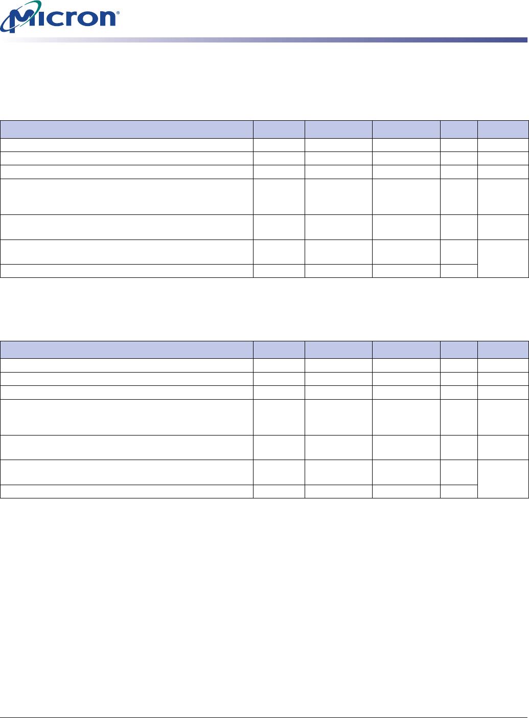
Table 5: DC Electrical Characteristics and Operating Conditions (H version)
VDD = +1.8V ±0.1V VDDQ = +1.8V ±0.1V
Notes: 1, 5, 6; please refer to the 256Mb: x32 Mobile SDRAM data sheet for all notes.
Parameter/Condition Symbol MIN MAX Units Notes
Supply Voltage
VDD/VDDQ 1.7 1.9 V
Input High Voltage: Logic 1; All inputs
VIH
0.8 x VDDQ
VDDQ + 0.3 V22
Input Low Voltage: Logic 0; All inputs
VIL -0.3 0.3 V 22
Input Leakage Current:
Any input 0V V
IN VDD
(All other balls not under test = 0V)
II -1.0 1.0 µA
Output Leakage Current: DQs are disabled; 0V V
OUT
V
DDQ
IOZ -1.5 1.55 µA
Output Levels:
Output High Voltage (IOUT = -4mA)
V
OH 0.9 x VDDQ V
Output Low Voltage (IOUT = 4mA)
V
OL –0.2V
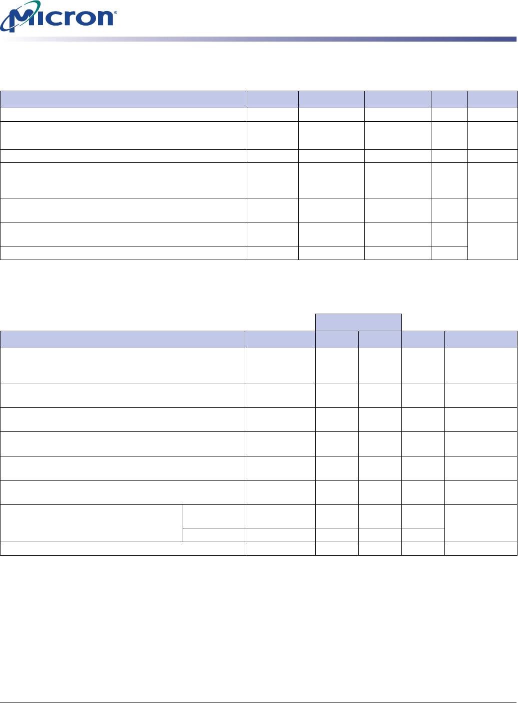
Table 6: IDD Specifications and Conditions (LC version)
VDD = +3.3V ±0.3V, VDDQ = +3.3V ±0.3V
Notes: 1, 5, 6, 11, 13; please refer to the 256Mb: x32 Mobile SDRAM data sheet for all notes.
MAX
Parameter/Condition Symbol -8 -10 Units Notes
Operating Current: Active Mode; Burst = 2; READ or
WRITE;
t
RC =
t
RC (MIN)
I
DD1 210 185 mA 3, 18, 19, 28
Standby Current: Power-Down Mode; All banks idle; CKE
= LOW
I
DD2N 800 800 µA 32
Standby Current: Power-Down Mode; All banks idle; CKE
= HIGH
I
DD2NS 60 60 mA
Standby Current: Active Mode; CKE = HIGH; CS# = HIGH;
All banks active after
t
RCD met; No accesses in progress
I
DD3NS 80 80 mA 3, 12, 19, 28
Standby Current: Active Mode; CKE = LOW; CS# = HIGH;
All banks active; No accesses in progress
I
DD3N 60 60 mA
Operating Current: Burst Mode; Continuous burst; READ
or WRITE; All banks active, half DQs toggling every cycle.
I
DD4 165 140 mA 3, 18, 19, 28
Auto Refresh Current
CKE = HIGH; CS# = HIGH
t
RFC =
t
RFC
(MIN)
I
DD5 300 250 mA 3, 12, 18, 19,
28, 29
t
RFC = 7.8µs
I
DD65.05.0mA
Deep power down
I
ZZ 20 20 µA

MT48H16M32L2F5-10 TR

Mfr. #:
Manufacturer:
Micron
Description:
IC DRAM 512M PARALLEL 90VFBGA
Lifecycle:
New from this manufacturer.
Delivery:
DHL FedEx Ups TNT EMS
Payment:
T/T Paypal Visa MoneyGram Western Union