Sensitive SCRs Data Sheets
http://www.littelfuse.com E5 - 4 ©2004 Littelfuse, Inc.
+1 972-580-7777 Thyristor Product Catalog
Specific Test Conditions
di/dt — Maximum rate-of-change of on-state current; I
GT
= 50 mA pulse
width 15 µsec with 0.1 µs rise time
dv/dt — Critical rate-of-rise of forward off-state voltage
I
2
t — RMS surge (non-repetitive) on-state current for period of 8.3 ms
for fusing
I
DRM
and I
RRM
— Peak off-state current at V
DRM
and V
RRM
I
GT
— DC gate trigger current V
D
= 6 V dc; R
L
= 100
I
GM
— Peak gate current
I
H
— DC holding current; initial on-state current = 20 mA
I
T
— Maximum on-state current
I
TSM
— Peak one-cycle forward surge current
P
G(AV)
— Average gate power dissipation
P
GM
— Peak gate power dissipation
t
gt
— Gate controlled turn-on time gate pulse = 10 mA; minimum
width = 15 µS with rise time 0.1 µs
t
q
— Circuit commutated turn-off time
V
DRM
and V
RRM
— Repetitive peak off-state forward and reverse voltage
V
GRM
— Peak reverse gate voltage
V
GT
— DC gate trigger voltage; V
D
= 6 V dc; R
L
= 100
V
TM
— Peak on-state voltage
General Notes
Teccor 2N5064 and 2N6565 Series devices conform to all JEDEC
registered data. See specifications table on pages E5 - 2 and
E5 - 3.
The case lead temperature (
T
C
or T
L
) is measured as shown on
dimensional outline drawings in the “Package Dimensions” section
of this catalog.
All measurements (except I
GT
) are made with an external resistor
R
GK
= 1 k unless otherwise noted.
All measurements are made at 60 Hz with a resistive load at an
ambient temperature of +25 °C unless otherwise specified.
Operating temperature (T
J
) is -65 °C to +110 °C for EC Series
devices, -65 °C to +125 °C for 2N Series devices, -40 °C to
+125 °C for “TCR” Series, and -40 °C to +110 °C for all others.
Storage temperature range (T
S
) is -65 °C to +150 °C for TO-92
devices, -40 °C to +150 °C for TO-202 and Compak devices, and
-40 °C to +125 °C for all others.
Lead solder temperature is a maximum of +230 °C for 10 seconds
maximum 1/16" (1.59 mm) from case.
TYPE
Part Number
I
T
V
DRM
&
V
RRM
I
GT
I
DRM
&
I
RRM
V
TM
Isolated Non-isolated
TO-220 TO-202
TO-251
V-Pak
TO-252
D-Pak
(1)
Amps
Volts
(2) (12)
µAmps
(20) (21)
µAmps
(3) (10)
Volts
See “Package Dimensions” section for variations. (11)
I
T(RMS)
I
T(AV)
T
C
=
25 °C
T
C
=
110 °C
MAX MAX MIN MAX MAX MAX MAX
6A
S2006LS2 S2006FS21 S2006VS2 S2006DS2 6 3.8 200 200 5 250 1.6
S4006LS2 S4006FS21 S4006VS2 S4006DS2 6 3.8 400 200 5 250 1.6
S6006LS2 S6006FS21 S6006VS2 S6006DS2 6 3.8 600 200 5 250 1.6
S2006LS3 S2006FS31 S2006VS3 S2006DS3 6 3.8 200 500 5 250 1.6
S4006LS3 S4006FS31 S4006VS3 S4006DS3 6 3.8 400 500 5 250 1.6
S6006LS3 S6006FS31 S6006VS3 S6006DS3 6 3.8 600 500 5 250 1.6
8A
S2008LS2 S2008FS21 S2008VS2 S2008DS2 8 5.1 200 200 5 250 1.6
S4008LS2 S4008FS21 S4008VS2 S4008DS2 8 5.1 400 200 5 250 1.6
S6008LS2 S6008FS21 S6008VS2 S6008DS2 8 5.1 600 200 5 250 1.6
S2008LS3 S2008FS31 S2008VS3 S2008DS3 8 5.1 200 500 5 250 1.6
S4008LS3 S4008FS31 S4008VS3 S4008DS3 8 5.1 400 500 5 250 1.6
S6008LS3 S6008FS31 S6008VS3 S6008DS3 8 5.1 600 500 5 250 1.6
10 A
S2010LS2 S2010FS21 S2010VS2 S2010DS2 10 6.4 200 200 5 250 1.6
S4010LS2 S4010FS21 S4010VS2 S4010DS2 10 6.4 400 200 5 250 1.6
S6010LS2 S6010FS21 S6010VS2 S6010DS2 10 6.4 600 200 5 250 1.6
S2010LS3 S2010FS31 S2010VS3 S2010DS3 10 6.4 200 500 5 250 1.6
S4010LS3 S4010FS31 S4010VS3 S4010DS3 10 6.4 400 500 5 250 1.6
S6010LS3 S6010FS31 S6010VS3 S6010DS3 10 6.4 600 500 5 250 1.6
K
A
G
K
A
G
A
A
A
G
K
A
A
K
G
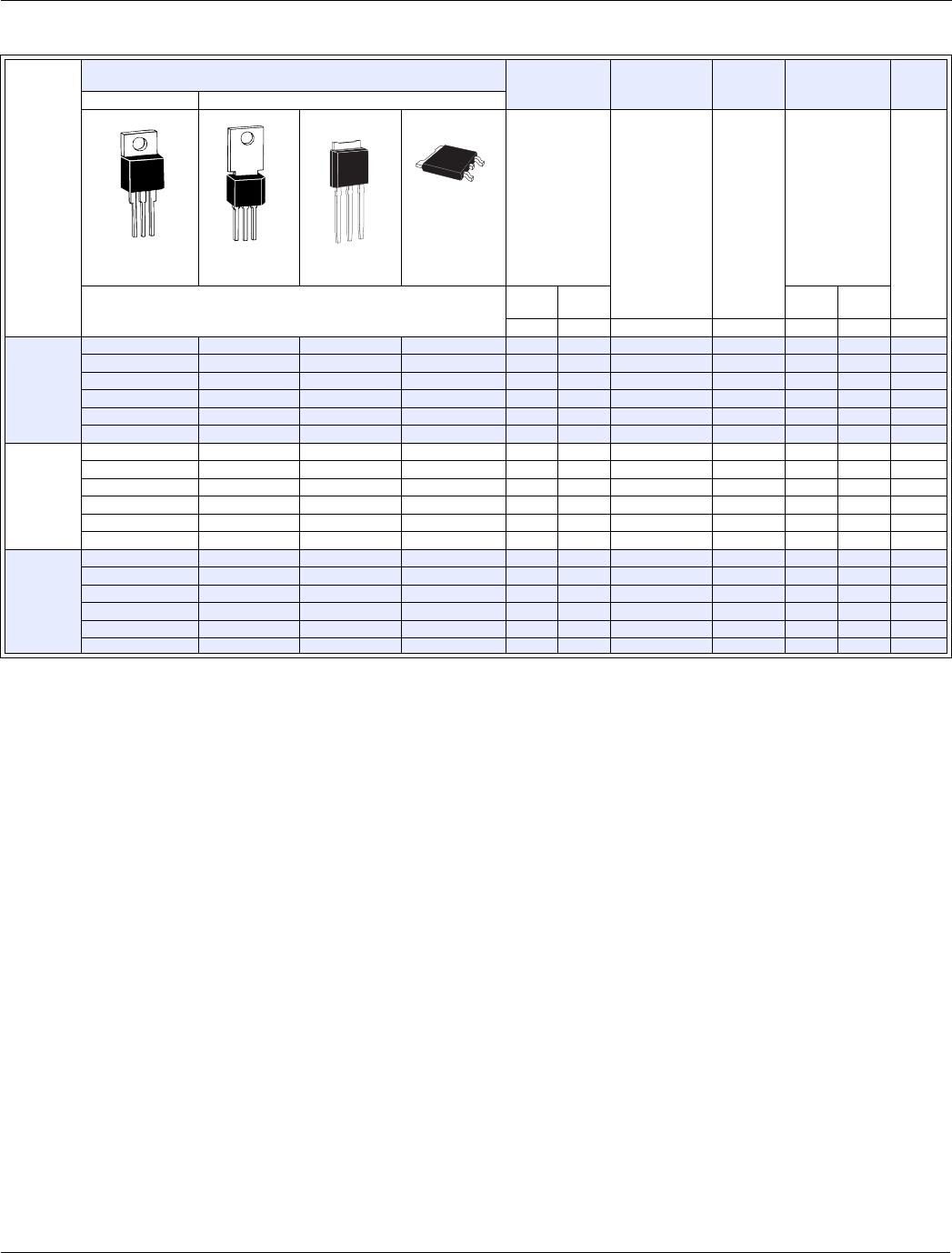
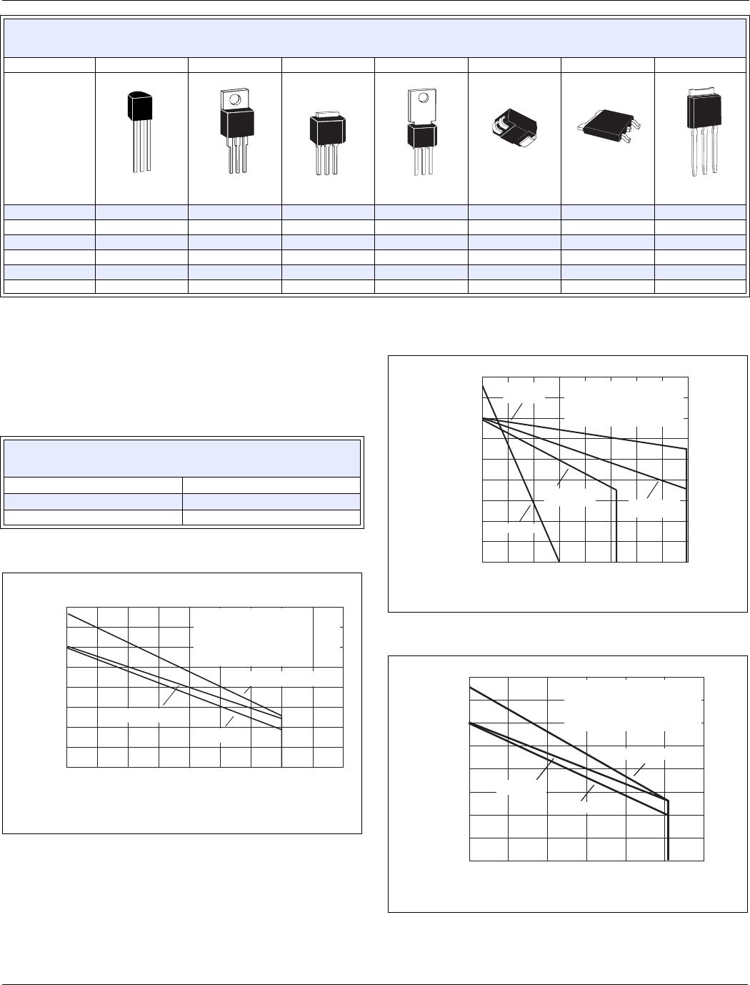
Data Sheets Sensitive SCRs
©2004 Littelfuse, Inc. E5 - 5 http://www.littelfuse.com
Thyristor Product Catalog +1 972-580-7777
Electrical Specifications Notes
(1) See Figure E5.1 through Figure E5.9 for current ratings at
specified operating temperatures.
(2) See Figure E5.10 for I
GT
versus T
C
or T
L
.
(3) See Figure E5.11 for instantaneous on-state current (i
T
) versus on-
state voltage (v
T
) TYP.
(4) See Figure E5.12 for V
GT
versus T
C
or T
L
.
(5) See Figure E5.13 for I
H
versus T
C
or T
L
.
(6) For more than one full cycle, see Figure E5.14.
(7) 0.8 A to 4 A devices also have a pulse peak forward current on-
state rating (repetitive) of 75 A. This rating applies for operation at
60 Hz, 75 °C maximum tab (or anode) lead temperature, switching
from 80 V peak, sinusoidal current pulse width of 10 µs minimum,
15 µs maximum. See Figure E5.20 and Figure E5.21.
(8) See Figure E5.15 for t
gt
versus I
GT
.
(9) Test conditions as follows:
– T
C
or T
L
80 °C, rectangular current waveform
– Rate-of-rise of current 10 A/µs
– Rate-of-reversal of current 5A/µs
– I
TM
= 1 A (50 µs pulse), Repetition Rate = 60 pps
– V
RRM
= Rated
– V
R
= 15 V minimum, V
DRM
= Rated
– Rate-of-rise reapplied forward blocking voltage = 5 V/µs
– Gate Bias = 0 V, 100 (during turn-off time interval)
(10) Test condition is maximum rated RMS current except TO-92
devices are 1.2 A
PK
; T106/T107 devices are 4 A
PK
.
(11) See package outlines for lead form configurations. When ordering
special lead forming, add type number as suffix to part number.
(12) V
D
= 6 V dc, R
L
= 100 (See Figure E5.19 for simple test circuit
for measuring gate trigger voltage and gate trigger current.)
(13) See Figure E5.1 through Figure E5.9 for maximum allowable case
temperature at maximum rated current.
(14) I
GT
= 500 µA maximum at T
C
= -40 °C for T106 devices
(15) I
H
= 10 mA maximum at T
C
= -65 °C for 2N5064 Series and
2N6565 Series devices
(16) I
H
= 6 mA maximum at T
C
= -40 °C for T106 devices
(17) Pulse Width 10 µs
(18) I
GT
= 350 µA maximum at T
C
= -65 °C for 2N5064 Series and
2N6565 Series devices
(19) Latching current can be higher than 20 mA for higher I
GT
types.
Also, latching current can be much higher at -40 °C. See Figure
E5.18.
(20) T
C
or T
L
= T
J
for test conditions in off state
(21) I
DRM
and I
RRM
= 50 µA for 2N5064 and 100 µA for 2N6565 at
125 °C
(22) TO-92 devices specified at -65 °C instead of -40 °C
(23) T
C
= 110 °C
V
GT
I
H
I
GM
V
GRM
P
GM
P
G(AV)
I
TSM
dv/dt di/dt
t
gt
t
q
l
2
t
(4) (12) (22)
Volts
(5) (19)
mAmps
(17)
Amps Volts
(17)
Watts Watts
(6) (13)
Amps
Volts/µSec
Amps/µSec
(8)
µSec
(9)
µSec Amps
2
Sec
T
C
=
-40 °C
T
C
=
25 °C
T
C
=
110 °C T
C
= 110 °C
MAX MAX MIN 60/50 Hz TYP TYP MAX
1 0.8 0.25 6 1 6 1 0.1 100/83 10 100 4 50 41
1 0.8 0.25 6 1 6 1 0.1 100/83 8 100 4 50 41
1 0.8 0.25 6 1 6 1 0.1 100/83 8 100 4 50 41
1 0.8 0.25 8 1 6 1 0.1 100/83 10 100 5 45 41
1 0.8 0.25 8 1 6 1 0.1 100/83 8 100 5 45 41
1 0.8 0.25 8 1 6 1 0.1 100/83 8 100 5 45 41
10.80.2561610.1100/8310 100 45041
10.80.2561610.1100/838 100 45041
10.80.2561610.1100/838 100 45041
10.80.2581610.1100/8310 100 54541
10.80.2581610.1100/838 100 54541
10.80.2581610.1100/838 100 54541
1 0.8 0.25 6 1 6 1 0.1 100/83 10 100 4 50 41
1 0.8 0.25 6 1 6 1 0.1 100/83 8 100 4 50 41
1 0.8 0.25 6 1 6 1 0.1 100/83 8 100 4 50 41
1 0.8 0.25 8 1 6 1 0.1 100/83 10 100 5 45 41
1 0.8 0.25 8 1 6 1 0.1 100/83 8 100 5 45 41
1 0.8 0.25 8 1 6 1 0.1 100/83 8 100 5 45 41
Sensitive SCRs Data Sheets
http://www.littelfuse.com E5 - 6 ©2004 Littelfuse, Inc.
+1 972-580-7777 Thyristor Product Catalog
*Mounted on 1 cm
2
copper foil surface; two-ounce copper foil
Electrical Isolation
Teccor’s isolated sensitive SCRs will withstand a minimum high
potential test of 2500 V ac rms from leads to mounting tab over
the device's operating temperature range. The following table
shows other standard and optional isolation ratings.
*UL Recognized File #E71639
**For 4000 V isolation, use “V” suffix in part number.
Figure E5.1 Maximum Allowable Case Temperature versus
RMS On-state Current
Figure E5.2 Maximum Allowable Case Temperature versus
RMS On-state Current
Figure E5.3 Maximum Allowable Case Temperature versus
Average On-state Current
Thermal Resistance (Steady State)
R
θJC
[R
θ JA
] °C/W (TYPICAL)
Package Code
ELF2FCDV
Type
TO-92 TO-220 TO-202
Type 2, 4, & 41
TO-202
Type 1 & 3
Compak TO-252
D-Pak
TO-251
V-Pak
0.8 A 75 [160] 60*
1.5 A 50 [160]
4.0 A 10 [100] 6.2 [80] 3.0 3.8 [85]
6.0 A 4.0 [65] 4.3 1.8 2.4
8.0 A 3.4 3.9 1.5 2.1
10.0 A 3.0 3.4 1.45 1.72
Electrical Isolation *
from Leads to Mounting Tab
VACRMS TO-220
2500
Standard
4000
Optional **
50
60
70
80
90
100
110
120
130
CURRENT WAVEFORM: Sinusoidal
LOAD: Resistive or Inductive
CONDUCTION ANGLE: 180
˚
CASE TEMPERATURE: Measured
as Shown on Dimensional Drawing
RMS On-State Current [
I
T(RMS)
] – Amps
Maximum Allowable
Case Temperature (T
C
) – ˚C
Compak
0.1 0.2 0.3 0.4 0.5 0.6 0.7 0.8 0.9 1.0
EC Series
JEDEC 2N Series
0 0.5 1.0 1.5 2.0 2.5 3.0 3.5 4.0
40
50
60
70
80
90
100
110
120
130
CURRENT WAVEFORM: Sinusoidal
LOAD: Resistive or Inductive
CONDUCTION ANGLE: 180˚
CASE TEMPERATURE: Measured
as Shown on Dimensional Drawing
RMS On-state Current [
I
T(RMS)
] – Amps
Maximum Allowable Case Temperature (
T
C
) – ˚C
2.6
4 A TO-251
and TO-252
T106 and T107
Type 1 and 3
T106 and T107
Type 2 and 4
TCR22 Devices
0 0.1 0.2 0.3 0.4 0.5 0.6
50
60
70
80
90
100
110
120
130
CURRENT WAVEFORM: Sinusoidal
LOAD: Resistive or Inductive
CONDUCTION ANGLE: 180˚
CASE TEMPERATURE: Measured
as Shown on Dimensional Drawing
Average On-state Current [
I
T(AV)
] – Amps
Maximum Allowable Case Temperature (
T
C
) – ˚C
0.51
Compak
EC Series
JEDEC 2N Series

S2006FS211

Mfr. #:
Manufacturer:
Littelfuse
Description:
SCRs 6A 200V Sensing
Lifecycle:
New from this manufacturer.
Delivery:
DHL FedEx Ups TNT EMS
Payment:
T/T Paypal Visa MoneyGram Western Union