LTC4444
3
4444fb
Note 1: Stresses beyond those listed under Absolute Maximum Ratings
may cause permanent damage to the device. Exposure to any Absolute
Maximum Rating condition for extended periods may affect device
reliability and lifetime.
Note 2: The LTC4444 is tested under pulsed load conditions such that
T
J
≈ T
A
. The LTC4444E is guaranteed to meet specifications from 0°C
to 85°C junction temperature. Specifications over the –40°C to 125°C
operating junction temperature range are assured by design, charac-
terization and correlation with statistical process controls. The LTC4444I
is guaranteed over the –40°C to 125°C operating temperature range, the
LTC4444H is guaranteed over the –40°C to 150°C operating temperature
range and the LTC4444MP is tested and guaranteed over the full –55°C to
150°C operating junction temperature range. High junction temperatures
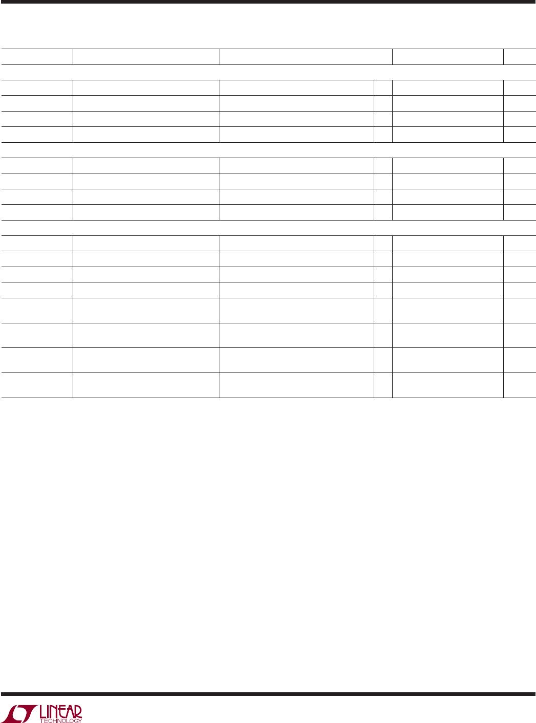
ELECTRICAL CHARACTERISTICS
The l denotes the specifications which apply over the full operating junction
temperature range, otherwise specifications are at T
A
= 25°C (Note 2). V
CC
= V
BOOST
= 12V, V
TS
= GND = 0V, unless otherwise noted.
SYMBOL PARAMETER CONDITIONS MIN TYP MAX UNITS
High Side Gate Driver Output (TG)
V
OH(TG)
TG High Output Voltage I
TG
= –10mA, V
OH(TG)
= V
BOOST
– V
TG
0.7 V
V
OL(TG)
TG Low Output Voltage I
TG
= 100mA, V
OL(TG)
= V
TG
–V
TS
l
120 250 mV
I
PU(TG)
TG Peak Pull-Up Current
l
1.7 2.5 A
R
DS(TG)
TG Pull-Down Resistance
l
1.2 2.5
Ω
Low Side Gate Driver Output (BG)
V
OH(BG)
BG High Output Voltage I
BG
= –10mA, V
OH(BG)
= V
CC
– V
BG
0.7 V
V
OL(BG)
BG Low Output Voltage I
BG
= 100mA
l
55 125 mV
I
PU(BG)
BG Peak Pull-Up Current
l
23 A
R
DS(BG)
BG Pull-Down Resistance
l
0.55 1.25
Ω
Switching Time [BINP (TINP) is Tied to Ground While TINP (BINP) is Switching. Refer to Timing Diagram]
t
PLH(TG)
TG Low-High Propagation Delay
l
25 50 ns
t
PHL(TG)
TG High-Low Propagation Delay
l
22 45 ns
t
PLH(BG)
BG Low-High Propagation Delay
l
19 40 ns
t
PHL(BG)
BG High-Low Propagation Delay
l
14 35 ns
t
r(TG)
TG Output Rise Time 10% – 90%, C
L
= 1nF
10% – 90%, C
L
= 10nF
8
80
ns
ns
t
f(TG)
TG Output Fall Time 10% – 90%, C
L
= 1nF
10% – 90%, C
L
= 10nF
5
50
ns
ns
t
r(BG)
BG Output Rise Time 10% – 90%, C
L
= 1nF
10% – 90%, C
L
= 10nF
6
60
ns
ns
t
f(BG)
BG Output Fall Time 10% – 90%, C
L
= 1nF
10% – 90%, C
L
= 10nF
3
30
ns
ns
degrade operating lifetimes; operating lifetime is derated for junction
temperatures greater than 125°C. Note that the maximum ambient
temperature consistent with these specifications is determined by specific
operating conditions in conjunction with board layout, the rated package
thermal impedance and other environmental factors.
Note 3: The junction temperature (T
J
, in °C) is calculated from the ambient
temperature (T
A
, in °C) and power dissipation (P
D
, in watts) according to
the formula:
T
J
= T
A
+ (P
D
• θ
JA
)
where θ
JA
(in °C/W) is the package thermal impedance.
Note 4: Failure to solder the exposed back side of the MS8E package to the
PC board will result in a thermal resistance much higher than 40°C/W.