LTC4444
9
4444fb
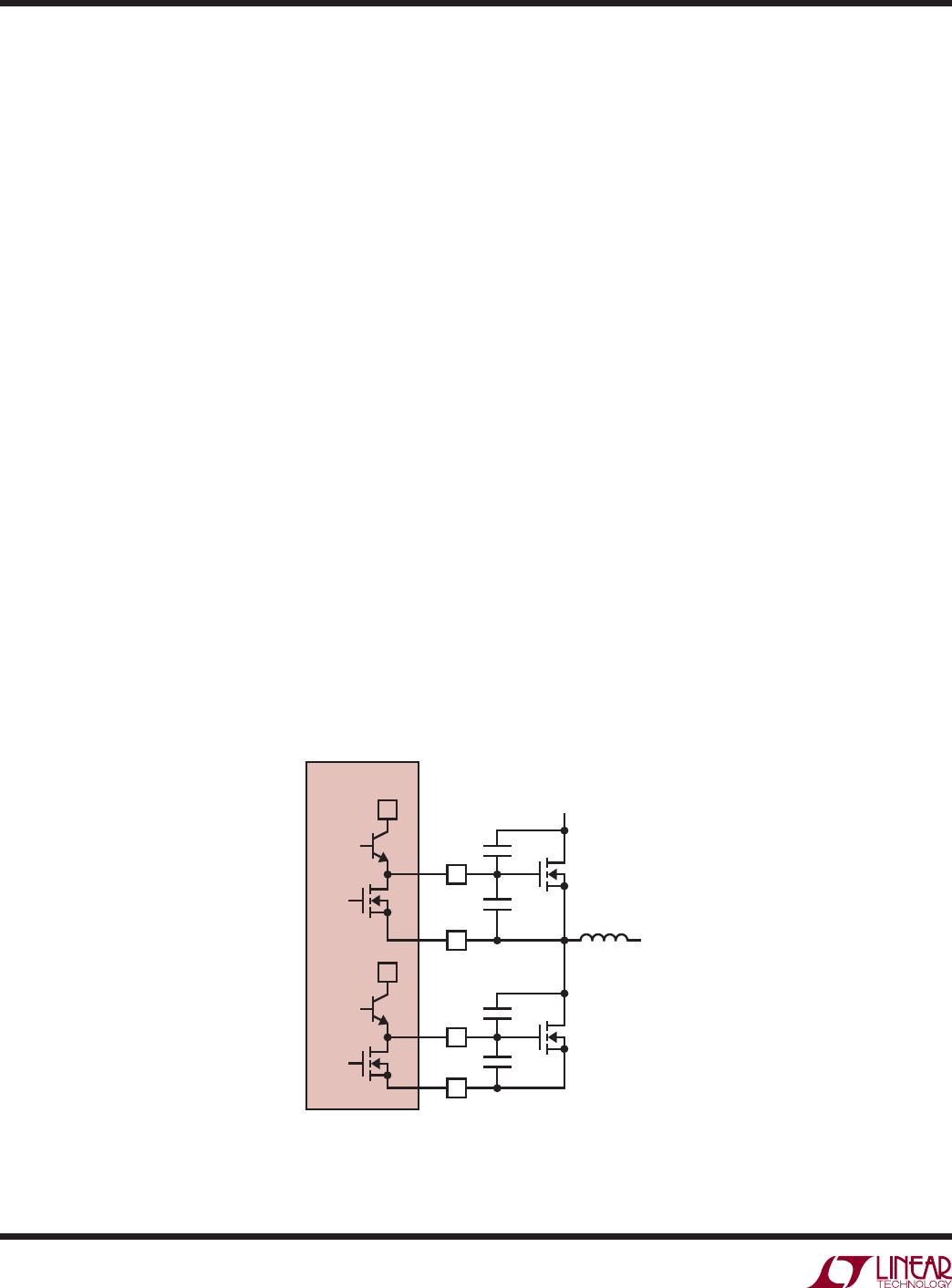
pull-down on the driver outputs is the prevention of cross-
conduction current. For example, when BG turns the low
side (synchronous) power MOSFET off and TG turns the
high side power MOSFET on, the voltage on the TS pin
will rise to V
IN
very rapidly. This high frequency positive
voltage transient will couple through the C
GD
capacitance
of the low side power MOSFET to the BG pin. If there is
an insufficient pull-down on the BG pin, the voltage on
the BG pin can rise above the threshold voltage of the low
side power MOSFET, momentarily turning it back on. With
both the high side and low side MOSFETs conducting,
significant cross-conduction current will flow through the
MOSFETs from V
IN
to ground and will cause substantial
power loss. A similar effect occurs on TG due to the C
GS
and C
GD
capacitances of the high side MOSFET.
The powerful output driver of the LTC4444 reduces the
switching losses of the power MOSFET, which increase
with transition time. The LTC4444’s high side driver is
capable of driving a 1nF load with 8ns rise and 5ns fall
times using a bootstrapped supply voltage V
BOOST-TS
of
12V while its low side driver is capable of driving a 1nF
load with 6ns rise and 3ns fall times using a supply volt-
age V
CC
of 12V.
Undervoltage Lockout (UVLO)
The LTC4444 contains an undervoltage lockout detector
that monitors V
CC
supply. When V
CC
falls below 6.15V,
the output pins BG and TG are pulled down to GND and
TS, respectively. This turns off both external MOSFETs.
When V
CC
has adequate supply voltage, normal operation
will resume.
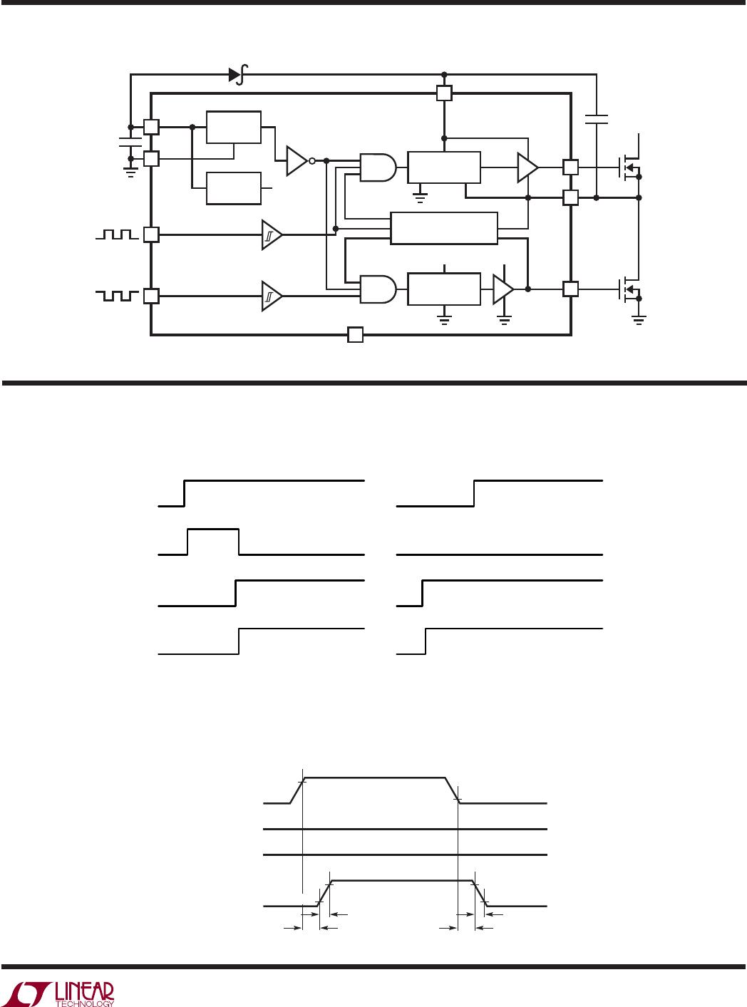
Adaptive Shoot-Through Protection
Internal adaptive shoot-through protection circuitry moni-
tors the voltages on the external MOSFETs to ensure that
they do not conduct simultaneously. This feature improves
efficiency by eliminating cross-conduction current from
flowing from the V
IN
supply through both of the MOSFETs
to ground during a switch transition. If both TINP and
BINP are high at the same time, BG will be kept off and
TG will be turned on (refer to the Timing Diagram). If BG
is still high when TINP turns on, TG will not be turned on
until BG goes low.
When TINP turns off, the adaptive shoot-through protec-
tion circuitry monitors the level of the TS pin. BG can be
turned on if the TS pin goes low. If the TS pin stays high,
BG will be turned on 150ns after TINP turns off.
APPLICATIONS INFORMATION
Power Dissipation
To ensure proper operation and long-term reliability, the
LTC4444 must not operate beyond its maximum tem-
perature rating. Package junction temperature can be
calculated by:
T
J
= T
A
+ P
D
(θ
JA
)
where:
T
J
= Junction temperature
T
A
= Ambient temperature
P
D
= Power dissipation
θ
JA
= Junction-to-ambient thermal resistance
Power dissipation consists of standby and switching
power losses:
P
D
= P
DC
+ P
AC
+ P
QG
where:
P
DC
= Quiescent power loss
P
AC
= Internal switching loss at input frequency, f
IN
P
QG
= Loss due turning on and off the external MOSFET
with gate charge QG at frequency f
IN
The LTC4444 consumes very little quiescent current. The
DC power loss at V
CC
= 12V and V
BOOST-TS
= 12V is only
(350µA)(12V) = 4.2mW.
OPERATION