VS-ST110S04P2VPBF

VS-ST110SPbF Series
www.vishay.com
Vishay Semiconductors
Revision: 11-Mar-14
4
Document Number: 94393
For technical questions within your region: DiodesAmericas@vishay.com
, DiodesAsia@vishay.com, DiodesEurope@vishay.com
THIS DOCUMENT IS SUBJECT TO CHANGE WITHOUT NOTICE. THE PRODUCTS DESCRIBED HEREIN AND THIS DOCUMENT
ARE SUBJECT TO SPECIFIC DISCLAIMERS, SET FORTH AT www.vishay.com/doc?91000
Fig. 1 - Current Ratings Characteristics Fig. 2 - Current Ratings Characteristics
Fig. 3 - On-State Power Loss Characteristics
Fig. 4 - On-State Power Loss Characteristics
80
90
100
110
120
130
0 20406080100120
Maximum Allowable Case Temperature (°C)
30°
60°
90°
120°
180°
Average On-state Current (A)
Conduction Angle
ST110S Series
R (DC) = 0.195 K/W
thJC
80
90
100
110
120
130
0 20 40 60 80 100 120 140 160 180
DC
30°
60°
90°
120°
180°
Average On-state Current (A)
Maximum Allowable Case Temperature (°C)
Conduction Period
ST110S Series
R (DC) = 1.95 K/W
thJC
25 50 75 100 125
Maximum Allowable Ambient Temperature (°C)
R
=
0
.
1
K
/
W
-
D
e
l
t
a
R
0
.
2
K
/
W
0
.
3
K
/
W
0
.
4
K
/
W
0
.
5
K
/
W
0
.
6
K
/
W
1
K
/
W
0
.
8
K
/
W
1
.
2
K
/
W
t
h
S
A
0
20
40
60
80
100
120
140
160
020406080100120
180°
120°
90°
60°
30°
RMS Limit
Conduction Angle
Maximum Average On-state Power Loss (W)
Average On-state Current (A)
ST110S Series
T = 125°C
J
25 50 75 100 125
Maximum Allowable Ambient Temperature (°C)
R
=
0
.
1
K/
W
-
D
e
l
t
a
R
t
h
S
A
0
.
2
K
/
W
0
.
3
K
/
W
0
.
4
K
/
W
0
.
6
K
/
W
0
.
8
K
/
W
1
K
/
W
0
.
5
K
/
W
1
.
2
K
/
W
0
20
40
60
80
100
120
140
160
180
200
220
0 20 40 60 80 100 120 140 160 180
DC
180°
120°
90°
60°
30°
RMS Limit
Conduction Period
Maximum Average On-state Power Loss (W)
Average On-state Current (A)
ST110S Series
T = 125°C
J
VS-ST110SPbF Series
www.vishay.com
Vishay Semiconductors
Revision: 11-Mar-14
5
Document Number: 94393
For technical questions within your region: DiodesAmericas@vishay.com
, DiodesAsia@vishay.com, DiodesEurope@vishay.com
THIS DOCUMENT IS SUBJECT TO CHANGE WITHOUT NOTICE. THE PRODUCTS DESCRIBED HEREIN AND THIS DOCUMENT
ARE SUBJECT TO SPECIFIC DISCLAIMERS, SET FORTH AT www.vishay.com/doc?91000
Fig. 5 - Maximum Non-Repetitive Surge Current Fig. 6 - Maximum Non-Repetitive Surge Current
Fig. 7 - On-State Voltage Drop Characteristics
Fig. 8 - Thermal Impedance Z
thJC
Characteristic
1000
1200
1400
1600
1800
2000
2200
2400
110100
Number Of Equal Amplitude Half Cycle Current Pulses (N)
Peak Half Sine Wave On-state Current (A)
Initial T = 125°C
@ 60 Hz 0.0083 s
@ 50 Hz 0.0100 s
ST110S Series
J
At Any Rated Load Condition And With
Rated V Applied Following Surge.
RRM
1000
1200
1400
1600
1800
2000
2200
2400
2600
2800
0.01 0.1 1 10
Pulse Train Duration (s)
Maximum Non Repetitive Surge Current
Versus Pulse Train Duration. Control
Of Conduction May Not Be Maintained.
Peak Half Sine Wave On-state Current (A)
Initial T = 125°C
No Voltage Reapplied
Rated V Reapplied
J
RRM
ST110S Series
Instantaneous On-state Voltage (V)
Instantaneous On-state Current (A)
10
100
1000
10000
0.5 1.5 2.5 3.5 4.5
Tj = 25˚C
Tj = 125˚C
ST110S Series
0.001
0.01
0.1
1
0.001 0.01 0.1 1 10
Square Wave Pulse Duration (s)
thJC
Transient Thermal Impedance Z (K/W)
ST110S Series
Steady State Value
R = 0.195 K/W
(DC Operation)
thJC
VS-ST110SPbF Series
www.vishay.com
Vishay Semiconductors
Revision: 11-Mar-14
6
Document Number: 94393
For technical questions within your region: DiodesAmericas@vishay.com
, DiodesAsia@vishay.com, DiodesEurope@vishay.com
THIS DOCUMENT IS SUBJECT TO CHANGE WITHOUT NOTICE. THE PRODUCTS DESCRIBED HEREIN AND THIS DOCUMENT
ARE SUBJECT TO SPECIFIC DISCLAIMERS, SET FORTH AT www.vishay.com/doc?91000
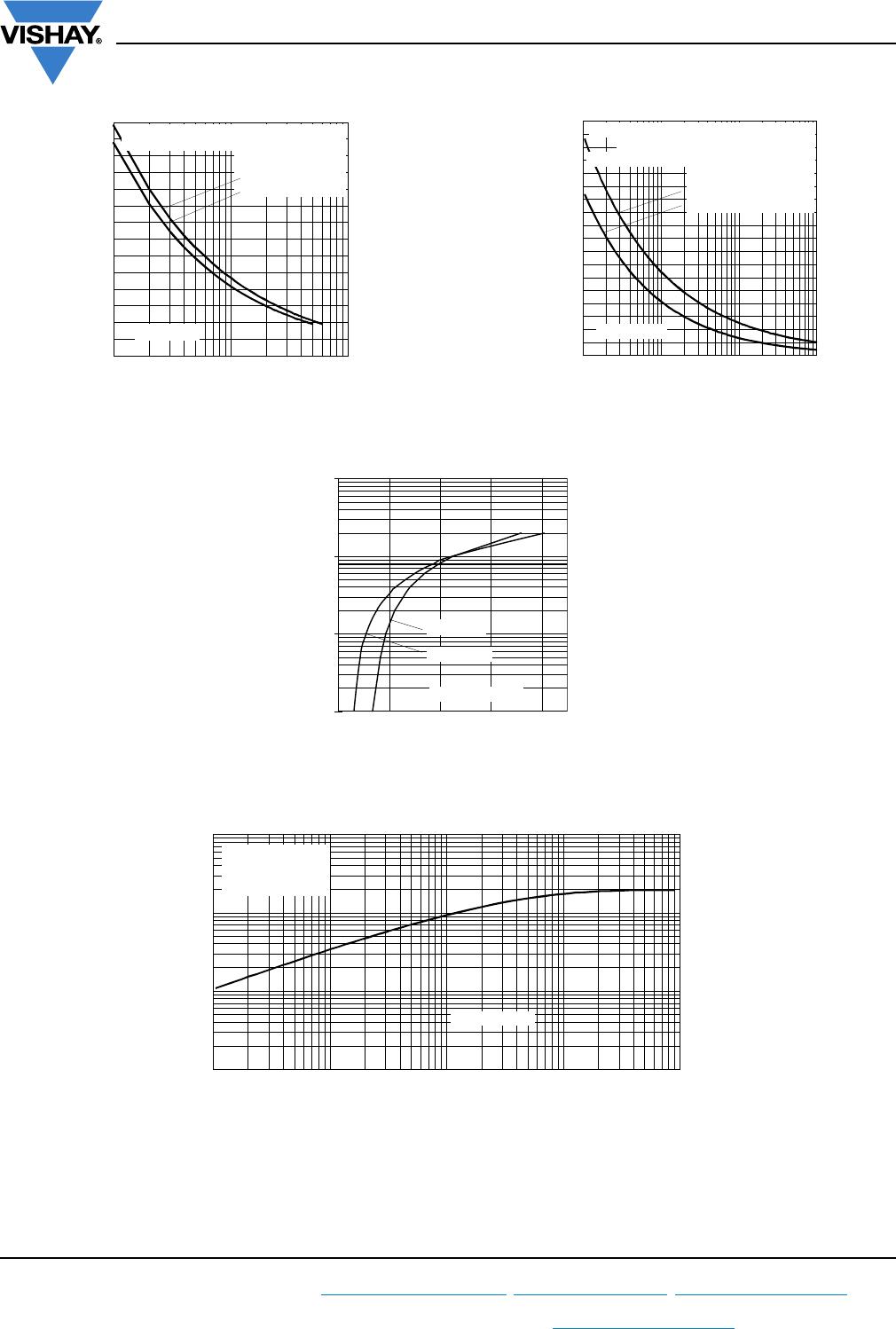
Fig. 9 - Gate Characteristics
ORDERING INFORMATION TABLE
LINKS TO RELATED DOCUMENTS
Dimensions www.vishay.com/doc?95078
0.1
1
10
100
0.001 0.01 0.1 1 10 100
VGD
IGD
(b)
(a)
Tj=25 °C
Tj=125 °C
Tj=-40 °C
(1) (2)
(3)
Instantaneous Gate Current (A)
Instantaneous Gate Voltage (V)
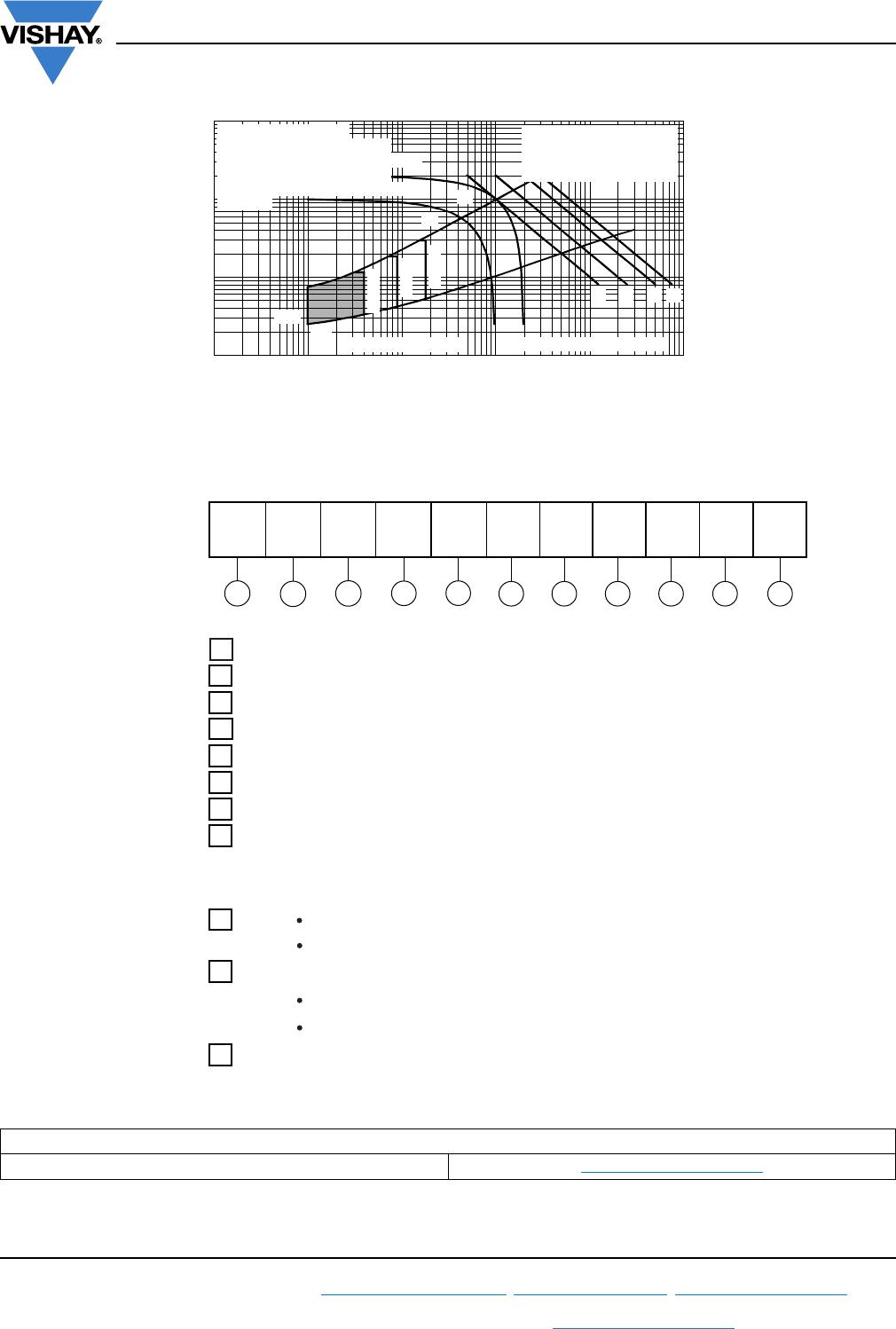
a) Recommended load line for
b) Recommended load line for
<=30% rated di/dt : 10V, 10ohms
Frequency Limited by PG(AV)
rated di/dt : 20V, 10ohms; tr<=1 µs
tr<=1 µs
(1) PGM = 10W, tp = 4ms
(2) PGM = 20W, tp = 2ms
(3) PGM = 40W, tp = 1ms
(4) PGM = 60W, tp = 0.66ms
Device: ST110S Series
Rectangular gate pulse
(4)
- Thyristor
2
- Essential part marking
3
- 0 = Converter grade
4
11
10
- S = Compression bonding stud
8
- V = Glass-metal seal (only up to 1200 V)
5
- Voltage code x 100 = V
RRM
(see Voltage Ratings table)
6
- P = Stud base 20UNF threads
7
- 0 = Eyelet terminals (gate and auxiliary cathode leads)
1 = Fast-on terminals (gate and auxiliary cathode leads)
2 = Flag terminals (for cathode and gate terminals)
9
- Critical dV/dt:
None = Ceramic housing (over 1200 V)
None = 500 V/µs (standard value)
L = 1000 V/µs (special selection)
Device code
51 32 4 6 7 8 9 10 11
STVS- 11 0 S 16 P 0 V L PbF
1 - Vishay Semiconductors product
- None = Standard production
- PbF = Lead (Pb)-free

VS-ST110S04P2VPBF

Mfr. #:
Manufacturer:
Vishay Semiconductors
Description:
SCRs Thyristors - TO-83/94 COM RD-e3
Lifecycle:
New from this manufacturer.
Delivery:
DHL FedEx Ups TNT EMS
Payment:
T/T Paypal Visa MoneyGram Western Union