VS-VSK.166..PbF, VS-VSK.196..PbF, VS-VSK.236..PbF Series
www.vishay.com
Vishay Semiconductors
Revision: 29-Sep-15
9
Document Number: 94357
For technical questions within your region: DiodesAmericas@vishay.com
, DiodesAsia@vishay.com, DiodesEurope@vishay.com
THIS DOCUMENT IS SUBJECT TO CHANGE WITHOUT NOTICE. THE PRODUCTS DESCRIBED HEREIN AND THIS DOCUMENT
ARE SUBJECT TO SPECIFIC DISCLAIMERS, SET FORTH AT www.vishay.com/doc?91000
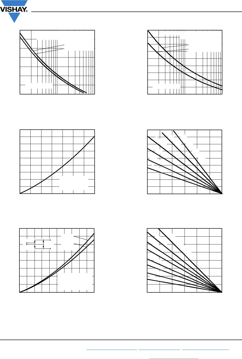
Fig. 27 - On-State Power Loss Characteristics
Fig. 28 - On-State Voltage Drop Characteristics
Fig. 29 - On-State Voltage Drop Characteristics
Fig. 30 - On-State Voltage Drop Characteristics
Fig. 31 - Thermal Impedance Z
thJC
Characteristics
0
500
2500
2000
1500
1000
Maximum Total Power Loss (W)
Total Output Current (A)
200100 300 400
700
500 600
0
120°
(Rect)
3 x VSK.236.. Series
Three phase bridge
Connected
T
J
= 150 °C
+
-
~
0
500
2500
2000
1500
1000
Maximum Total Power Loss (W)
Maximum Allowable Ambient Temperature (°C)
5025 75 100
150
125
0
0.04 K/W
0.06 K/W
0.1 K/W
0.16 K/W
0.3 K/W
0.7 K/W
R
thSA
= 0.02 K/W - ΔR
1
100
10
10 000
1000
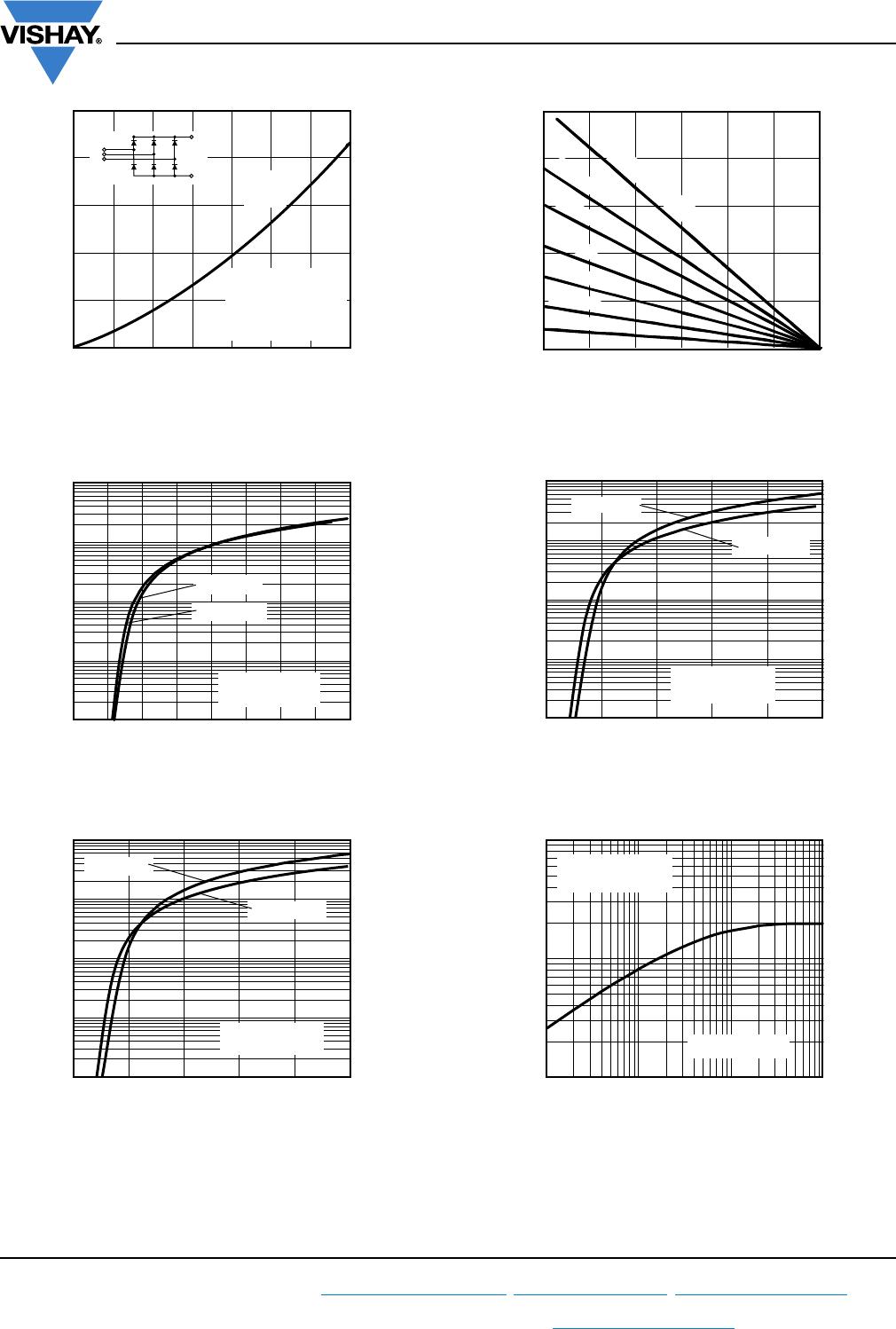
Instantaneous On-State Current (A)
Instantaneous On-State Voltage (V)
0.5 1.0 1.5 2.0 3.02.5 3.5
4.0
0
T
J
= 25 °C
VSK.166.. Series
Per junction
T
J
= 150 °C
1
100
10
10 000
1000
Instantaneous On-State Current (A)
Instantaneous On-State Voltage (V)
1.0 2.0 3.0 4.0
5.0
0
T
J
= 25 °C
T
J
= 150 °C
VSK.196.. Series
Per junction
1
100
10
10 000
1000
Instantaneous On-State Current (A)
Instantaneous On-State Voltage (V)
1.0 2.0 3.0 4.0 5.0
0
T
J
= 25 °C
T
J
= 150 °C
VSK.236.. Series
Per junction
0.01
0.1
1
Z
thJC
- Transient Thermal Impedance
Square Wave Pulse Duration (s)
10.1
10
0.01
VSK.166.. Series
Steady state value
(DC operation)