LTC4359
1
Rev D
For more information www.analog.comDocument Feedback
TYPICAL APPLICATION
FEATURES DESCRIPTION
Ideal Diode Controller with
Reverse Input Protection
The LT C
®
4359 is a positive high voltage ideal diode control-
ler that drives an external N-channel MOSFET to replace
a Schottky diode. It controls the for
ward-voltage drop
across the MOSFET to ensure smooth current delivery
without oscillation even at light loads. If a power source
fails or is shorted, a fast turn-off minimizes reverse cur
-
rent transients. A shutdown mode is available to reduce
the quiescent current to
9μA for load switch and 14µA for
ideal diode applications.
When used in high current diode applications, the LTC4359
reduces power consumption, heat dissipation, voltage loss
and PC board area. With its wide operating voltage range,
the ability to withstand reverse input voltage, and high
temperature rating, the LTC4359 satisfies the demanding
requirements of both automotive and telecom applications.
The LTC4359 also easily ORs power sources in systems
with redundant supplies.
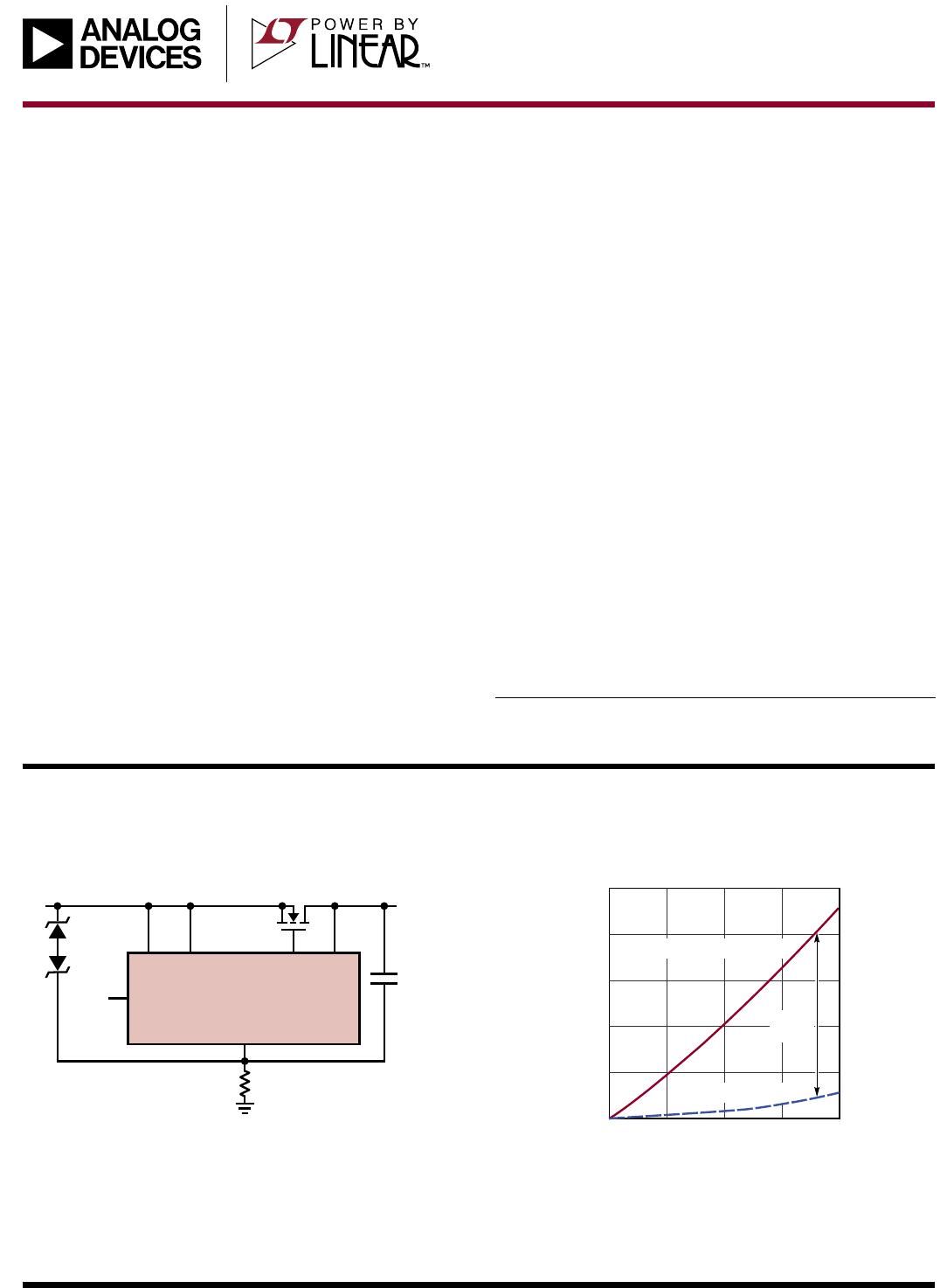
12V, 20A Automotive Reverse-Battery Protection Power Dissipation vs Load Current
APPLICATIONS
n
Reduces Power Dissipation by Replacing a Power
Schottky Diode
n
Wide Operating Voltage Range: 4V to 80V
n
Reverse Input Protection to – 40V
n
Low 9µA Shutdown Current
n
Low 150μA Operating Current
n
Smooth Switchover without Oscillation
n
Controls Single or Back-to-Back N-Channel MOSFETs
n
Available in 6-Pin (2mm × 3mm) DFN, 8-Lead MSOP
and 8-Lead SO Packages
n
Automotive Battery Protection
n
Redundant Power Supplies
n
Supply Holdup
n
Telecom Infrastructure
n
Computer Systems/Servers
n
Solar Systems
All registered trademarks and trademarks are the property of their respective owners.
4359 TA01
LTC4359
V
SS
SHDN
IN SOURCE OUT
47nF
1k
GATE
BSC028N06NS
SMAT70A
70V
SMAJ24A
24V
V
IN
12V
V
OUT
TO LOAD
CURRENT (A)
0
POWER DISSIPATION (W)
4
8
6
20
4359 TA01a
2
0
5
10
15
10
SCHOTTKY DIODE (SBG2040CT)
POWER
SAVED
MOSFET (BSC028N06NS)
LTC4359
2
Rev D
For more information www.analog.com
ABSOLUTE MAXIMUM RATINGS
IN, SOURCE, SHDN ................................... 40V to 100V
OUT (Note 3) ................................................2V to 100V
IN OUT ..................................................100V to 100V
IN SOURCE .................................................1V to 80V
GATE – SOURCE (Note 4) .........................0.3V to +10V
(Notes 1, 2)
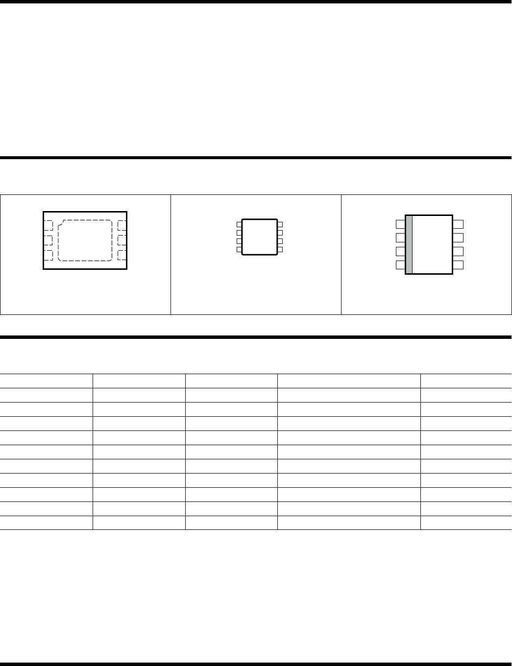
TOP VIEW
V
SS
SHDN
IN
OUT
GATE
SOURCE
DCB PACKAGE
6-LEAD (2mm × 3mm) PLASTIC DFN
T
JMAX
= 150°C, θ
JA
= 64°C/W
EXPOSED PAD (PIN 7) PCB V
SS
CONNECTION OPTIONAL
4
5
7
6
3
2
1
1
2
3
4
GATE
SOURCE
NC
IN
8
7
6
5
OUT
NC
V
SS
SHDN
TOP VIEW
MS8 PACKAGE
8-LEAD PLASTIC MSOP
T
JMAX
= 150°C, θ
JA
= 163°C/W
1
2
3
4
8
7
6
5
TOP VIEW
OUT
NC
V
SS
SHDN
GATE
SOURCE
NC
IN
S8 PACKAGE
8-LEAD PLASTIC SO
T
JMAX
= 150°C, θ
JA
= 130°C/W
PIN CONFIGURATION
ORDER INFORMATION
Operating Ambient Temperature Range
LTC4359C ................................................ 0°C to 70°C
LTC4359I ............................................. 40°C to 85°C
LTC4359H .......................................... 40°C to 125°C
Storage Temperature Range .................. 65°C to 150°C
Lead Temperature (Soldering, 10 sec)
MS, SO Packages ............................................. 300°C
TAPE AND REEL (MINI) TAPE AND REEL PART MARKING* PACKAGE DESCRIPTION TEMPERATURE RANGE
LTC4359CDCB#TRMPBF LTC4359CDCB#TRPBF LFKF 6-Lead (2mm × 3mm) Plastic DFN 0°C to 70°C
LTC4359IDCB#TRMPBF LTC4359IDCB#TRPBF LFKF 6-Lead (2mm × 3mm) Plastic DFN –40°C to 85°C
LTC4359HDCB#TRMPBF LTC4359HDCB#TRPBF LFKF 6-Lead (2mm × 3mm) Plastic DFN –40°C to 125°C
TUBE TAPE AND REEL PART MARKING* PACKAGE DESCRIPTION TEMPERATURE RANGE
LTC4359CMS8#PBF LTC4359CMS8#TRPBF LTFKD 8-Lead Plastic MSOP 0°C to 70°C
LTC4359IMS8#PBF LTC4359IMS8#TRPBF LTFKD 8-Lead Plastic MSOP –40°C to 85°C
LTC4359HMS8#PBF LTC4359HMS8#TRPBF LTFKD 8-Lead Plastic MSOP –40°C to 125°C
LTC4359CS8#PBF LTC4359CS8#TRPBF 4359 8-Lead Plastic SO 0°C to 70°C
LTC4359IS8#PBF LTC4359IS8#TRPBF 4359 8-Lead Plastic SO –40°C to 85°C
LTC4359HS8#PBF LTC4359HS8#TRPBF 4359 8-Lead Plastic SO –40°C to 125°C
Consult ADI Marketing for parts specified with wider operating temperature ranges. *The temperature grade is identified by a label on the shipping container.
For more information on lead free part marking, go to: http://www.linear.com/leadfree/
For more information on tape and reel specifications, go to: http://www.linear.com/tapeandreel/. Some packages are available in 500 unit reels through
designated sales channels with #TRMPBF suffix.
http://www.linear.com/product/LTC4359#orderinfo
LTC4359
3
Rev D
For more information www.analog.com
Note 1: Stresses beyond those listed under Absolute Maximum Ratings
may cause permanent damage to the device. Exposure to any Absolute
Maximum Rating condition for extended periods may affect device
reliability and lifetime.
Note 2. All currents into pins are positive; all voltages are referenced to
V
SS
unless otherwise specified.
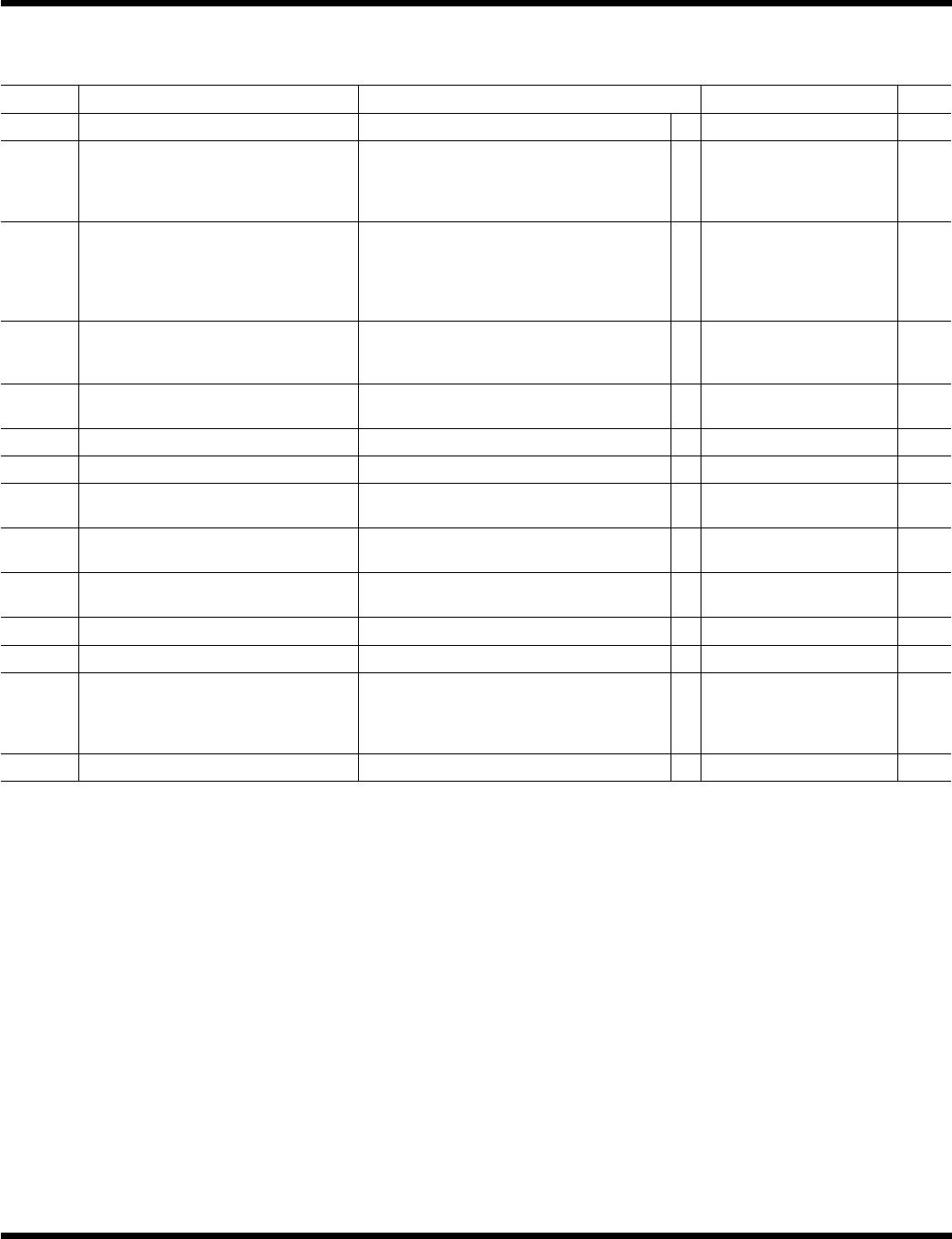
SYMBOL PARAMETER CONDITIONS MIN TYP MAX UNITS
V
IN
Operating Supply Range
l
4 80 V
I
IN
IN Current IN = 12V
IN = OUT = 12V, SHDN = 0V
IN = OUT = 24V, SHDN = 0V
IN = −40V
l
l
l
l
0
150
9
15
–15
200
20
30
–40
µA
µA
µA
µA
I
OUT
OUT Current IN = 12V, In Regulation
IN = 12V, ∆V
SD
= −1V
IN = OUT = 12V, SHDN = 0V
IN = OUT = 24V, SHDN = 0V
OUT = 12V, IN = SHDN = 0V
l
l
l
l
l
3
5
120
0.8
0.8
6
7.5
220
3
3
12
µA
µA
µA
µA
µA
I
SOURCE
SOURCE Current IN = 12V, ∆V
SD
= −1V
IN = SOURCE = 12V, SHDN = 0V
SOURCE = –40V
l
l
l
1
–0.4
150
4
–0.8
200
15
–1.5
µA
µA
mA
V
GATE
Gate Drive (GATE–SOURCE) IN = 4V, I
GATE
= 0, −1µA
IN = 8V to 80V; I
GATE
= 0, –1µA
l
l
4.5
10
5.5
12
15
15
V
V
V
SD
Source-Drain Regulation Voltage (IN –OUT) ∆V
GATE
= 2.5V
l
20 30 45 mV
I
GATE(UP)
Gate Pull-Up Current GATE = IN, ∆V
SD
= 0.1V
l
–6 –10 –14 µA
I
GATE(DOWN)
Gate Pull-Down Current Fault Condition, ∆V
GATE
= 5V, ∆V
SD
= −1V
Shutdown Mode, ∆V
GATE
= 5V, ∆V
SD
= 0.7V
l
l
70
0.6
130 180 mA
mA
t
OFF
Gate Turn-Off Delay Time ∆V
SD
= 0.1V to −1V, ∆V
GATE
< 2V,
C
GATE
= 0pF
l
0.3 0.5 µs
t
ON
Gate Turn-On Delay Time IN = 12V, SOURCE = OUT = 0V, SHDN = 0V to 2V
∆V
GATE
> 4.5V, C
GATE
= 0pF
200 µs
V
SHDN(TH)
SHDN Pin Input Threshold IN = 4V to 80V
l
0.6 1.2 2 V
V
SHDN(FLT)
SHDN Pin Float Voltage IN = 4V to 80V
l
0.6 1.75 2.5 V
I
SHDN
SHDN Pin Current SHDN = 0.5V, LTC4359I, LTC4359C
SHDN = 0.5V, LTC4359H
SHDN = −40V
Maximum Allowable Leakage, V
IN
= 4V
l
l
l
–1
–0.5
–0.4
3
–3
–0.8
100
5
–5
–1.5
µA
µA
mA
nA
V
SOURCE(TH)
Reverse SOURCE Threshold for GATE Off GATE = 0V, I
GATE(DOWN)
= 1mA
l
–0.9 –1.8 –2.7 V
The l denotes the specifications which apply over the full operating
temperature range, otherwise specifications are at T
A
= 25°C, IN = 12V, SOURCE = IN, unless otherwise noted.
Note 3. An internal clamp limits the OUT pin to a minimum of 100V above
V
SS
. Driving this pin with more current than 1mA may damage the device.
Note 4. An internal clamp limits the GATE pin to a minimum of 10V above
IN or 100V above V
SS
. Driving this pin to voltages beyond the clamp may
damage the device.
ELECTRICAL CHARACTERISTICS
LTC4359IMS8#PBF

Mfr. #:
Manufacturer:
Analog Devices / Linear Technology
Description:
Power Management Specialized - PMIC Ideal Diode Cntr w/ Reverse In Prot
Lifecycle:
New from this manufacturer.
Delivery:
DHL FedEx Ups TNT EMS
Payment:
T/T Paypal Visa MoneyGram Western Union