LTC4359
10
Rev D
For more information www.analog.com
Figure10 shows a +48V application with reverse input
protection where D5 is used instead of R1 to eliminate
the power dissipation and system ground current when the
input reverses to –48V. With –48V input and OUT powered
by another supply or held up by output capacitance, D2
(5.1V) and D3 (75V) prevent the LTC4359’s OUTIN pins
from exceeding the 100V absolute maximum rating. R2
limits the current into D1, D2 and D3 during a reverse input.
Paralleling Supplies
Multiple LTC4359s can be used to combine the outputs of
two or more supplies for redundancy or for droop sharing,
as shown in Figure5. For redundant supplies, the supply
with the highest output voltage sources most or all of the
load current. If this supplys output is quickly shorted to
ground while delivering load current, the flow of current
temporarily reverses and flows backwards through the
LTC4359’s MOSFET. The LTC4359 senses this reverse
current and activates a fast pull-down to quickly turn off
the MOSFET.
APPLICATIONS INFORMATION
LTC4359
V
SS
IN
D2A
SMAJ24CA
24V
OUT
C
OUTA
1.5µF
C
OUTB
1.5µF
GATE
Q1A
FDMS86101
12V
10A
BUS
R1A
1k
LTC4359
V
SS
IN
SOURCE
SHDN
SOURCE OUTGATE
Q1B
FDMS86101
PSA
V
INA
= 12V
RTNA
PSB
V
INB
= 12V
RTNB
D2B
SMAJ24CA
24V
4359 F05
R1B
1k
SHDN
Figure5. Redundant Power Supplies
If the other, initially lower, supply was not delivering any
load current at the time of the fault, the output falls until
the body diode of its ORing MOSFET conducts. Meanwhile,
the LTC4359 charges the MOSFET gate with 10µA until
the forward drop is reduced to 30mV. If this supply was
sharing load current at the time of the fault, its associated
ORing MOSFET was already driven partially on. In this case,
the LTC4359 will simply drive the MOSFET gate harder in
an effort to maintain a drop of 30mV.
Droop sharing can be accomplished if both power supply
output voltages and output impedances are nearly equal.
The 30mV regulation technique ensures smooth load
sharing between outputs without oscillation. The degree
of sharing is a function of MOSFET R
DS(ON)
, the output
impedance of the supplies and their initial output voltages.
Load Switching and Inrush Control
By adding a second MOSFET as shown in Figure6, the
LTC4359 can be used to control power flow in the for-
ward direction while retaining ideal diode behavior in the
reverse direction. The body diodes of Q1 and Q2 prohibit
ON OFF
4359 F06
LTC4359
V
SS
IN OUT
SHDN
GATESOURCE
Q1
FDMS86101
R4
10k
C1
10nF
V
IN
28V
Q2
FQA140N10
R3
10Ω
V
OUT
28V
10A
C
LOAD
C
OUT
1.5µF
R1
1k
D4
DDZ9699T
12V
D1
SMAJ58A
58V
D2
SMAJ24A
24V
Figure6. 28V Load Switch and Ideal
Diode with Reverse Input Protection
LTC4359
11
Rev D
For more information www.analog.com
APPLICATIONS INFORMATION
current flow when the MOSFETs are off. Q1 serves as the
ideal diode, while Q2 acts as a switch to control forward
power flow. On/off control is provided by the SHDN pin,
and C1 and R4 may be added if inrush control is desired.
When SHDN is driven high and provided V
IN
>V
OUT
+ 30mV,
GATE sources 10µA and gradually charges C1, pulling up
both MOSFET gates. Q2 operates as a source follower and
I
INRUSH
=
10µA C
LOAD
C1
If V
IN
<V
OUT
+ 30mV, the LTC4359 will be activated but
holds Q1 and Q2 off until the input exceeds the output by
30mV. In this way normal diode behavior of the circuit is
preserved, but with soft starting when the diode turns on.
When SHDN is pulled low, GATE pulls the MOSFET gates
down quickly to SOURCE turning off both forward and
reverse paths, and the input current is reduced to 9µA.
While C1 and R4 may be omitted if soft starting is not
needed, R3 is necessary to prevent MOSFET parasitic
oscillations and must be placed close to Q2.
Layout Considerations
Connect the IN, SOURCE and OUT pins as close as possible
to the MOSFET source and drain pins. Keep the traces to
the MOSFET wide and short to minimize resistive losses as
shown in Figure 7. Place surge suppressors and necessary
transient protection components close to the LTC4359
using short lead lengths.
For the DFN package, pin spacing may be a concern at
voltages greater than 30V. Check creepage and clearance
guidelines to determine if this is an issue. To increase the
effective pin spacing between high voltage and ground pins,
leave the exposed pad connection open. Use no-clean flux
to minimize PCB contamination.
Figures 8 through 18 show typical applications of the
LTC4359.
Figure 7a. Layout, DCB6 Package
Figure 7b. Layout, MS8/S8 Package
Figure8. 1.2V Diode–OR
4359 F07a
S
S
S
G
1
2
3
4
8
7
6
5
D
D
D
D
V
IN
OUT
LTC4359
GATE
IN
DCB6
4
5
7
6
3
2
1
V
OUT
SOURCE
MOSFET
LTC4359
S
S
S
G
1
2
3
4
8
7
6
5
D
D
D
D
MOSFET
GATE
IN
SOURCE
OUT
MS8/S8
4359 F07b
V
IN
V
OUT
LTC4359
V
SS
IN OUTGATE
Q1A
BSC011N03LS
–12V
–12V
V
OUT
1.2V
20A
R1A
1k
SOURCE
V
INA
1.2V
C
LOAD
C
OUTA
47nF
LTC4359
V
SS
IN OUTGATE
Q1B
BSC011N03LS
4359 F08
R1B
1k
SOURCE
V
INB
1.2V
C
OUTB
47nF
LTC4359
12
Rev D
For more information www.analog.com
TYPICAL APPLICATIONS
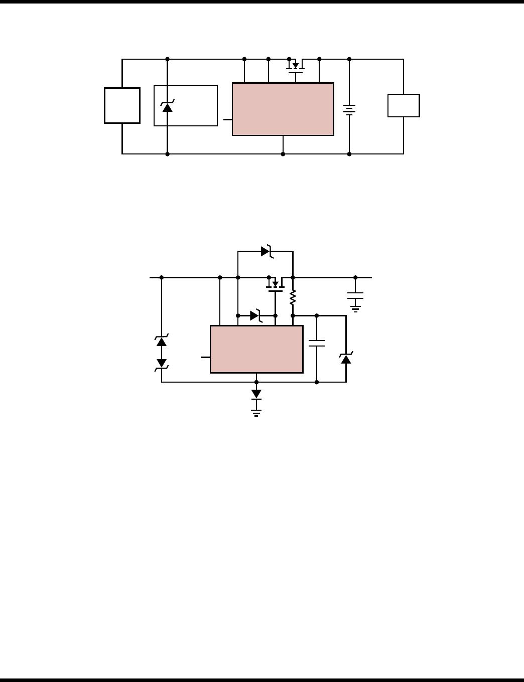
Figure9. Lossless Solar Panel Isolation
Figure10. 48V Ideal Diode with Reverse Input Protection
4359 F09
LTC4359
V
SS
SHDN
IN SOURCE OUTGATE
Q1
Si4874DY
+
12V
BATTERY
LOAD
SHUNT
REGULATOR
100W
SOLAR
PANEL
4359 F10
LTC4359
V
SS
SHDN
IN SOURCE OUTGATE
Q1
IPB200N25N3G
D6
SMCJ150A
150V
R2
2k
V
IN
48V
V
OUT
48V
10A
C
LOAD
C
OUT
47nF
D1
SMAT70A
70V
D2
MMSZ5231B
5.1V
D3
BZG03C75
75V
D5
S1B
D4
DDZ9699T
12V

LTC4359IMS8#PBF

Mfr. #:
Manufacturer:
Analog Devices / Linear Technology
Description:
Power Management Specialized - PMIC Ideal Diode Cntr w/ Reverse In Prot
Lifecycle:
New from this manufacturer.
Delivery:
DHL FedEx Ups TNT EMS
Payment:
T/T Paypal Visa MoneyGram Western Union