SN74GTL16616DLG4

SN74GTL16616DLG4
Mfr. #:
SN74GTL16616DLG4
Description:
Translation - Voltage Levels 17-Bit LVTTL-To-GTL/ GT=+ Univ Bus Trncvr
Lifecycle:
New from this manufacturer.
Datasheet:
SN74GTL16616DLG4 Datasheet
Delivery:
DHL FedEx Ups TNT EMS
Payment:
T/T Paypal Visa MoneyGram Western Union
ECAD Model:
More Information:
SN74GTL16616DLG4 more Information SN74GTL16616DLG4 Product Details
Product Attribute
Attribute Value
Manufacturer:
Texas Instruments
Product Category:
Translation - Voltage Levels
RoHS:
Y
Mounting Style:
SMD/SMT
Package / Case:
SSOP-56
Packaging:
Tube
Series:
74GTL
Brand:
Texas Instruments
Product Type:
Translation - Voltage Levels
Factory Pack Quantity:
1
Subcategory:
Logic ICs
Unit Weight:
0.024508 oz
Tags
SN74GTL16616DL, SN74GTL16616, SN74GTL1661, SN74GTL166, SN74GTL1, SN74G, SN74, SN7
Service Guarantees

We guarantee 100% customer satisfaction.

Quality Guarantees

We provide 90-360 days warranty.

If the items you received were not in perfect quality, we would be responsible for your refund or replacement, but the items must be returned in their original condition.
Our experienced sales team and tech support team back our services to satisfy all our customers.

we buy and manage excess electronic components, including excess inventory identified for disposal.
Email us if you have excess stock to sell.

Email: info@omo-ic.com
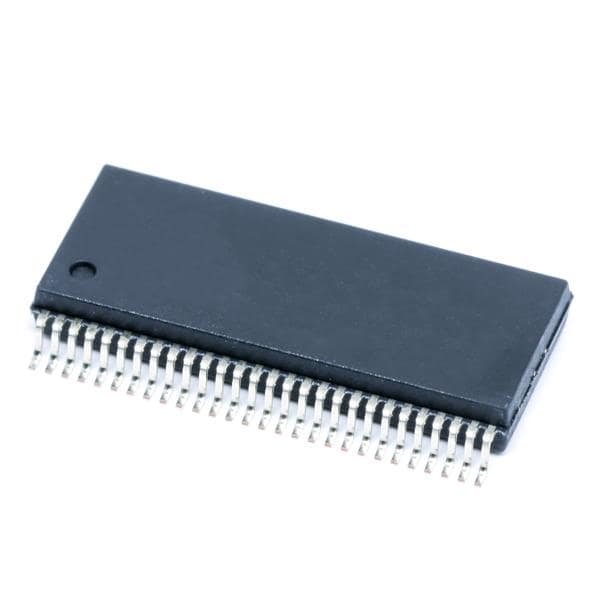
Step1: Vacuum Packaging with PL
Step1:
Vacuum Packaging with PL
Step2: Anti-Static Bag
Step2:
Anti-Static Bag
Step3: Packaging Boxes
Step3:
Packaging Boxes
***i-Key
IC UNIV BUS TXRX 17BIT 56SSOP
***as Instruments
The SN74GTL16616 is a 17-bit UBT™ transceiver that provides LVTTL-to-GTL/GTL+ and GTL/GTL+-to-LVTTL signal-level translation. Combined D-type flip-flops and D-type latches allow for transparent, latched, clocked, and clocked-enabled modes of data transfer identical to the '16601 function. Additionally, this device provides for a copy of CLKAB at GTL/GTL+ signal levels (CLKOUT) and conversion of a GTL/GTL+ clock to LVTTL logic levels (CLKIN). This device provides an interface between cards operating at LVTTL logic levels and a backplane operating at GTL/GTL+ signal levels. Higher-speed operation is a direct result of the reduced output swing (<1 V), reduced input threshold levels, and OEC™ circuitry. The user has the flexibility of using this device at either GTL (VTT = 1.2 V and VREF = 0.8 V) or the preferred higher noise margin GTL+ (VTT = 1.5 V and VREF = 1 V) signal levels. GTL+ is the Texas Instruments derivative of the Gunning Transceiver Logic (GTL) JEDEC standard JESD 8-3. The B port normally operates at GTL or GTL+ signal levels, while the A-port and control inputs are compatible with LVTTL logic levels and are 5-V tolerant. V REF is the reference input voltage for the B port. VCC (5 V) supplies the internal and GTL circuitry while VCC (3.3 V) supplies the LVTTL output buffers. Data flow in each direction is controlled by output-enable (OEAB\ and OEBA\), latch-enable (LEAB and LEBA), and clock (CLKAB and CLKBA) inputs. The clock can be controlled by the clock-enable (CEAB\ and CEBA\) inputs. For A-to-B data flow, the device operates in the transparent mode when LEAB is high. When LEAB is low, the A data is latched if CEAB\ is low and CLKAB is held at a high or low logic level. If LEAB is low, the A-bus data is stored in the latch/flip-flop on the low-to-high transition of CLKAB if CEAB\ also is low. When OEAB\ is low, the outputs are active. When OEAB\ is high, the outputs are in the high-impedance state. Data flow for B to A is similar to that of A to B, but uses OEBA\, LEBA, CLKBA, and CEBA\. This device is fully specified for partial-power-down applications using Ioff. The Ioff circuitry disables the outputs, preventing damaging current backflow through the device when it is powered down. Active bus-hold circuitry holds unused or undriven LVTTL inputs at a valid logic state. Use of pullup or pulldown resistors with the bus-hold circuitry is not recommended. To ensure the high-impedance state during power up or power down, OE\ should be tied to VCC through a pullup resistor; the minimum value of the resistor is determined by the current-sinking capability of the driver.
Image Part # Description
SN74GTL16622ADGGR

Mfr.#: SN74GTL16622ADGGR

OMO.#: OMO-SN74GTL16622ADGGR

Translation - Voltage Levels 3-Line to 8-Line Decoder/Demltplxr
SN74GTL1655DGGR

Mfr.#: SN74GTL1655DGGR

OMO.#: OMO-SN74GTL1655DGGR

Translation - Voltage Levels 16-Bit LVTTL To GTL/ GTL+ Univ Bus Trncvr
SN74GTL16616DLG4

Mfr.#: SN74GTL16616DLG4

OMO.#: OMO-SN74GTL16616DLG4

Translation - Voltage Levels 17-Bit LVTTL-To-GTL/ GT=+ Univ Bus Trncvr
SN74GTL1655DGGR/GTL1655

Mfr.#: SN74GTL1655DGGR/GTL1655

OMO.#: OMO-SN74GTL1655DGGR-GTL1655-1190

New and Original
SN74GTL1655DGGRE4

Mfr.#: SN74GTL1655DGGRE4

OMO.#: OMO-SN74GTL1655DGGRE4-1190

Translation - Voltage Levels 3-Line to 8-Line Decoder/Demltplx
SN74GTL16616DGGRG4

Mfr.#: SN74GTL16616DGGRG4

OMO.#: OMO-SN74GTL16616DGGRG4-1190

New and Original
SN74GTL16622ADGG

Mfr.#: SN74GTL16622ADGG

OMO.#: OMO-SN74GTL16622ADGG-1190

Registered Bus Transceiver, GTL/TVC Series, 2-Func, 9-Bit, True Output, BICMOS, PDSO64
SN74GTL16622DGGR

Mfr.#: SN74GTL16622DGGR

OMO.#: OMO-SN74GTL16622DGGR-1190

Registered Bus Transceiver, GTL/TVC Series, 2-Func, 9-Bit, True Output, BICMOS, PDSO64
SN74GTL16616DLR

Mfr.#: SN74GTL16616DLR

OMO.#: OMO-SN74GTL16616DLR-TEXAS-INSTRUMENTS

Translation - Voltage Levels 17-Bit LVTTL-To-GTL/ GT=+ Univ Bus Trncv
SN74GTL16612DGGR

Mfr.#: SN74GTL16612DGGR

OMO.#: OMO-SN74GTL16612DGGR-TEXAS-INSTRUMENTS

Translation - Voltage Levels 18Bit LVTTL/GTL/GTL+ Univ Bus Xcv
Availability
Stock:
Available
On Order:
3500
Enter Quantity:
Current price of SN74GTL16616DLG4 is for reference only, if you want to get best price, please submit a inquiry or direct email to our sales team sales@omo-ic.com
Start with
Newest Products
Top