SN74SSTEB32866ZWLR

SN74SSTEB32866ZWLR
Mfr. #:
SN74SSTEB32866ZWLR
Description:
Registers 1.5V/1.8V 25B Config Reg Buffer
Lifecycle:
New from this manufacturer.
Datasheet:
SN74SSTEB32866ZWLR Datasheet
Delivery:
DHL FedEx Ups TNT EMS
Payment:
T/T Paypal Visa MoneyGram Western Union
ECAD Model:
More Information:
SN74SSTEB32866ZWLR more Information SN74SSTEB32866ZWLR Product Details
Product Attribute
Attribute Value
Manufacturer:
Texas Instruments
Product Category:
Registers
RoHS:
Y
Logic Type:
CMOS
Logic Family:
SSTEB
Number of Circuits:
1
Maximum Clock Frequency:
410 MHz
Propagation Delay Time:
1.7 ns, 1.5 ns
High Level Output Current:
- 8 mA
Low Level Output Current:
8 mA
Supply Voltage - Max:
1.9 V
Supply Voltage - Min:
1.425 V
Minimum Operating Temperature:
- 40 C
Maximum Operating Temperature:
+ 85 C
Package / Case:
BGA-96
Packaging:
Reel
Height:
0.89 mm
Input Type:
Single-Ended
Length:
13.5 mm
Series:
SN74SSTEB32866
Width:
5.5 mm
Brand:
Texas Instruments
Mounting Style:
SMD/SMT
Number of Channels:
25
Number of Input Lines:
25
Number of Output Lines:
25
Moisture Sensitive:
Yes
Operating Supply Voltage:
1.5 V, 1.8 V
Polarity:
Non-Inverting
Product Type:
Registers
Reset Type:
Asynchronous
Factory Pack Quantity:
1000
Subcategory:
Logic ICs
Triggering Type:
Positive-Edge/Negative-Edge
Unit Weight:
0.006349 oz
Tags
SN74SST, SN74SS, SN74S, SN74, SN7
Service Guarantees

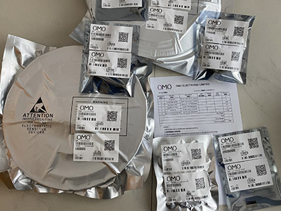
We guarantee 100% customer satisfaction.

Quality Guarantees

We provide 90-360 days warranty.

If the items you received were not in perfect quality, we would be responsible for your refund or replacement, but the items must be returned in their original condition.
Our experienced sales team and tech support team back our services to satisfy all our customers.

we buy and manage excess electronic components, including excess inventory identified for disposal.
Email us if you have excess stock to sell.

Email: info@omo-ic.com

Step1: Vacuum Packaging with PL
Step1:
Vacuum Packaging with PL
Step2: Anti-Static Bag
Step2:
Anti-Static Bag
Step3: Packaging Boxes
Step3:
Packaging Boxes
***as Instruments Inc.
This 25-bit 1:1 or 14-bit 1:2 configurable registered buffer is designed for 1.425-V to 1.9-V VCC operation. In the 1:1 pinout configuration, only one device per DIMM is required to drive nine SDRAM loads. In the 1:2 pinout configuration, two devices per DIMM are required to drive 18 SDRAM loads.
***AS INSRUMENTS
All inputs are SSTL_18, except the reset (RESET) and control (Cn) inputs, which are LVCMOS. All outputs are edge-controlled circuits optimized for unterminated DIMM loads and meets SSTL_18 and SSTL_15 specifications (depending on Supply voltage level), except the open-drain error (QERR) output.
***as Instruments Inc.
The SN74SSTEB32866 operates from a differential clock (CLK and CLK). Data are registered at the crossing of CLK going high and CLK going low.
***XS
The SN74SSTEB32866 accepts a parity bit from the memory controller on the parity bit (PAR_IN) input, compares it with the data received on the DIMM-independent D-inputs (D2-D3, D5-D6, D8-D25 when C0 = 0 and C1 = 0; D2-D3, D5-D6, D8-D14 when C0 = 0 and C1 = 1; or D1-D6, D8-D13 when C0 = 1 and C1 = 1) and indicates whether a parity error has occurred on the open-drain QERR pin (active low). The convention is even parity; i.e., valid parity is defined as an even number of ones across the DIMM-independent data inputs, combined with the parity input bit. To calculate parity, all DIMM-independent data inputs must be tied to a known logic state.
***OMO Electronic
When used as a single device, the C0 and C1 inputs are tied low. In this configuration, parity is checked on the PAR_IN input signal, which arrives one cycle after the input data to which it applies. Two clock cycles after the data are registered, the corresponding partial-parity-out (PPO) and QERR signals are generated.
***AS INSTRUMENT
When used in pairs, the C0 input of the first register is tied low, and the C0 input of the second register is tied high. The C1 input of both registers are tied high. Parity, which arrives one cycle after the data input to which it applies, is checked on the PAR_IN input signal of the first device. Two clock cycles after the data are registered, the corresponding PPO and QERR signals are generated on the second device. The PPO output of the first register is cascaded to the PAR_IN of the second SN74SSTEB32866. The QERR output of the first SN74SSTEB32866 is left floating, and the valid error information is latched on the QERR output of the second SN74SSTEB32866.
***
If an error occurs and the QERR output is driven low, it stays latched low for a minimum of two clock cycles or until RESET is driven low. If two or more consecutive parity errors occur, the QERR output is driven low and latched low for a clock duration equal to the parity-error duration or until RESET is driven low. The DIMM-dependent signals (DCKE, DCS, DODT, and CSR) are not included in the parity-check computation.
***AS INSTR
The C0 input controls the pinout configuration of the 1:2 pinout from register-A configuration (when low) to register-B configuration (when high). The C1 input controls the pinout configuration from 25-bit 1:1 (when low) to 14-bit 1:2 (when high). C0 and C1 should not be switched during normal operation. They should be hard-wired to a valid low or high level to configure the register in the desired mode. In the 25-bit 1:1 pinout configuration, the A6, D6, and H6 terminals are driven low and are do-not-use (DNU) pins.
***AS
In the DDR2 RDIMM application, RESET is specified to be completely asynchronous with respect to CLK and CLK. Therefore, no timing relationship can be ensured between the two. When entering reset, the register is cleared, and the data outputs are driven low quickly, relative to the time required to disable the differential input receivers. However, when coming out of reset, the register becomes active quickly, relative to the time required to enable the differential input receivers. As long as the data inputs are low, and the clock is stable during the time from the low-to-high transition of RESET until the input receivers are fully enabled, the design of the SN74SSTEB32866 ensures that the outputs remain low, thus ensuring there will be no glitches on the output.
***OMO Electronic
To ensure defined outputs from the register before a stable clock has been supplied, RESET must be held in the low state during power up.
***
The device supports low-power standby operation. When RESET is low, the differential input receivers are disabled, and undriven (floating) data, clock, and reference voltage (VREF) inputs are allowed. In addition, when RESET is low, all registers are reset and all outputs are forced low, except QERR. The LVCMOS RESET and Cn inputs always must be held at a valid logic high or low level.
***OMO Electronic
The device also supports low-power active operation by monitoring both system chip select (DCS and CSR) inputs and gates the Qn and PPO outputs from changing states when both DCS and CSR inputs are high. If either DCS or CSR input is low, the Qn and PPO outputs function normally. Also, if the internal low-power signal (LPS1) is high (one cycle after DCS and CSR go high), the device gates the QERR output from changing states. If LPS1 is low, the QERR output functions normally. The RESET input has priority over the DCS and CSR control and, when driven low, forces the Qn and PPO outputs low and forces the QERR output high. If the DCS control functionality is not desired, the CSR input can be hard-wired to ground, in which case the setup-time requirement for DCS is the same as for the other D data inputs. To control the low-power mode with DCS only, the CSR input should be pulled up to VCC through a pull-up resistor.
***AS INSRUMENTS
The two VREF pins (A3 and T3) are connected together internally by approximately 150. However, it is necessary to connect only one of the two VREF pins to the external VREF power supply. An unused VREF pin should be terminated with a VREF coupling capacitor.
Logic Solutions
OMO Electronic Logic Solutions offers a full spectrum of logic functions and technologies from the mature to the advanced, including bipolar, BiCMOS, and CMOS. TI's process technologies offer the logic performance and features required for modern logic designs, while maintaining support for more traditional logic products.Learn More
Part # Description Stock Price
SN74SSTEB32866ZWLR
DISTI # V72:2272_07360494
Registered Buffer Single 25-CH CMOS 96-Pin BGA T/R
RoHS: Compliant
1000
  • 75000:$6.8080
  • 30000:$6.8840
  • 15000:$6.9600
  • 6000:$7.0360
  • 3000:$7.1120
  • 1000:$7.1510
  • 500:$7.2270
  • 250:$8.1560
  • 100:$8.2420
  • 50:$9.7609
  • 25:$9.8640
  • 10:$9.9680
  • 1:$10.9030
SN74SSTEB32866ZWLR
DISTI # 296-24513-1-ND
IC BUFF CONFIG REG 25BIT 96BGA
RoHS: Compliant
Min Qty: 1
Container: Cut Tape (CT)
1105In Stock
  • 500:$7.8065
  • 100:$8.7756
  • 10:$10.3910
  • 1:$11.3100
SN74SSTEB32866ZWLR
DISTI # 296-24513-6-ND
IC BUFF CONFIG REG 25BIT 96BGA
RoHS: Compliant
Min Qty: 1
Container: Digi-Reel®
1105In Stock
  • 500:$7.8065
  • 100:$8.7756
  • 10:$10.3910
  • 1:$11.3100
SN74SSTEB32866ZWLR
DISTI # 296-24513-2-ND
IC BUFF CONFIG REG 25BIT 96BGA
RoHS: Compliant
Min Qty: 1000
Container: Tape & Reel (TR)
Temporarily Out of Stock
  • 1000:$6.9519
SN74SSTEB32866ZWLR
DISTI # 26560559
Registered Buffer Single 25-CH CMOS 96-Pin BGA T/R
RoHS: Compliant
1000
  • 1000:$7.1510
  • 500:$7.2270
  • 250:$8.1560
  • 100:$8.2420
  • 50:$9.7609
  • 25:$9.8640
  • 10:$9.9680
  • 1:$10.9030
SN74SSTEB32866ZWLR
DISTI # SN74SSTEB32866ZWLR
Registered Buffer Single 25-CH CMOS 96-Pin BGA T/R - Tape and Reel (Alt: SN74SSTEB32866ZWLR)
RoHS: Compliant
Min Qty: 1000
Container: Reel
Americas - 0
  • 1000:$6.7900
  • 2000:$6.6900
  • 4000:$6.6900
  • 6000:$6.6900
  • 10000:$6.6900
SN74SSTEB32866ZWLR1.5V/1.8V 25-Bit Configurable Registered Buffer With Address-Parity Test4000
  • 1000:$5.9400
  • 750:$6.0600
  • 500:$7.0000
  • 250:$8.0500
  • 100:$8.6300
  • 25:$9.6200
  • 10:$10.3000
  • 1:$11.4500
SN74SSTEB32866ZWLR
DISTI # 595-74SSTEB32866ZWLR
Registers 1.5V/1.8V 25B Config Reg Buffer
RoHS: Compliant
0
  • 1000:$6.9600
SN74SSTEB32866ZWLR 
RoHS: Not Compliant
177000
  • 1000:$6.8800
  • 500:$7.2400
  • 100:$7.5400
  • 25:$7.8700
  • 1:$8.4700
SN74SSTEB32866ZWLR
DISTI # C1S746202006706
Registered Buffer Single 25-CH CMOS 96-Pin BGA T/R
RoHS: Compliant
1000
  • 100:$8.2420
  • 50:$9.7609
  • 25:$9.8640
  • 10:$9.9680
  • 1:$10.9030
Image Part # Description
SN74SSTEB32866ZWLR

Mfr.#: SN74SSTEB32866ZWLR

OMO.#: OMO-SN74SSTEB32866ZWLR

Registers 1.5V/1.8V 25B Config Reg Buffer
SN74SSTEB32866ZWLR

Mfr.#: SN74SSTEB32866ZWLR

OMO.#: OMO-SN74SSTEB32866ZWLR-TEXAS-INSTRUMENTS

Registers 1.5V/1.8V 25B Config Reg Buffe
Availability
Stock:
Available
On Order:
5000
Enter Quantity:
Current price of SN74SSTEB32866ZWLR is for reference only, if you want to get best price, please submit a inquiry or direct email to our sales team sales@omo-ic.com
Start with
Newest Products
Top