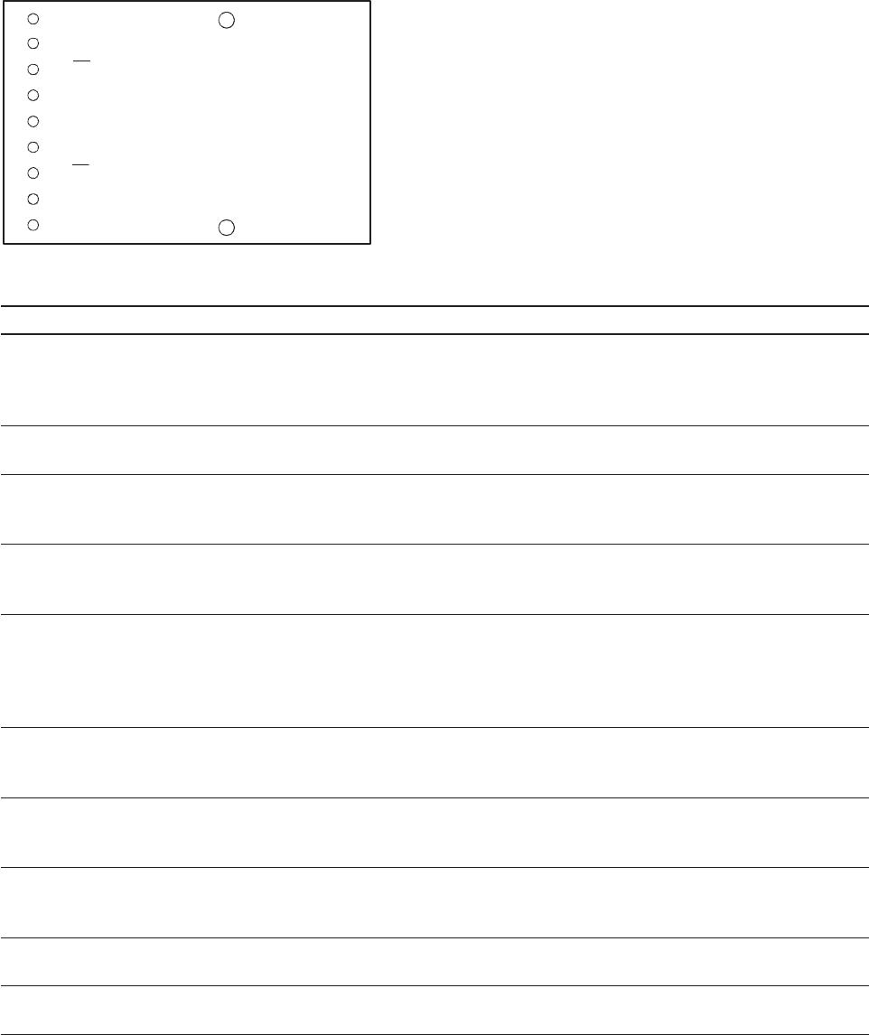
10
1 = V
EER
2 = RD
3 = RD
4 = SD
5 = V
CCR
6 = V
CCT
7 = TD
8 = TD
9 = V
EET
N/C
N/C
N/C = NO INTERNAL CONNECTION
(MOUNTING POSTS) - CONNECT
TO CHASSIS GROUND OR LEAVE
FLOATING, DO NOT CONNECT TO
SIGNAL GROUND.
TOP VIEW
Table 1. Pinout Table
Pin Symbol Functional Description
Mounting Studs The mounting studs are provided for transceiver mechanical attachment to the circuit boards, they are
embedded in the metalized plastic housing and are not connected to the transceiver internal circuit. They
should be soldered into plated-through holes on the printed circuit board and not connected to signal
ground.
1V
EER
Receiver Signal GroundDirectly connect this pin to receiver signal ground plane. Receiver V
EER
and trans-
mitter V
EET
can connect to a common circuit board ground plane.
2 RD+ Receiver Data Out
Terminate this high-speed, di erential, PECL output with standard PECL techniques at the follow-on
device input pin.
3 RD- Receiver Data Out Bar
Terminate this high-speed, di erential, PECL output with standard PECL techniques at the follow-on
device input pin.
4 SD Signal Detect
Normal input optical signal levels to the receiver result in a logic “1” output (V
OH
).Low input optical signal
levels to the receiver result in a fault condition indication shown by a logic “0” output (V
OL
).If Signal Detect
output is not used, leave it open-circuited.This Signal Detect output can be used to drive a PECL input on
an upstream circuit, such as, Signal Detect input or Loss of Signal-bar.
5V
CCR
Receiver Power Supply
Provide +5 V dc via the recommended receiver V
CCR
power supply  lter circuit.Locate the power supply
lter circuit as close as possible to the V
CCR
pin.
6V
CCT
Transmitter Power Supply
Provide +5 V dc via the recommended transmitter V
CCT
power supply  lter circuit.Locate the power supply
lter circuit as close as possible to the V
CCT
pin.
7 TD- Transmitter Data In Bar
Terminate this high-speed, di erential, Transmitter Data input with standard PECL techniques at the
transmitter input pin.
8 TD+ Transmitter Data InTerminate this high-speed, di erential, Transmitter Data input with standard PECL
techniques at the transmitter input pin.
9V
EET
Transmitter Signal GroundDirectly connect this pin to the transmitter signal ground plane. Transmitter
V
EET
and receiver V
EER
can connect to a common circuit board ground plane.
11
Absolute Maximum Ratings
Stresses in excess of the absolute maximum ratings can cause catastrophic damage to the device. Limits apply to each
parameter in isolation, all other parameters having values within the recommended operating conditions. It should
not be assumed that limiting values of more than one parameter can be applied to the product at the same time.
Exposure to the absolute maximum ratings for extended periods can adversely a ect device reliability.
Parameter Symbol Minimum Typical Maximum Unit Notes
Storage Temperature T
S
-40 +85 °C
Lead Soldering Temperature T
SOLD
+260 °C
Lead Soldering Time t
SOLD
10 sec.
Supply Voltage V
CC
-0.5 6.0 V
Data Input Voltage V
I
-0.5 V
CC
V
Transmitter Di erential Input Voltage V
D
1.6 V 1
Output Current I
D
50 mA
Relative Humidity RH 0 95 %
Recommended Operating Conditions
Parameter Symbol Minimum Typical Maximum Unit Notes
Ambient Operating Temperature T
A
0 +70 °C
Ambient Operating Temperature T
A
-40 +85 °C
Supply Voltage V
CC
4.75 5.25 V
Power Supply Rejection PSR 100 mV p-p 2
Transmitter Data Input Voltage - Low V
IL
-V
CC
-1.810 -1.475 V 3
Transmitter Data Input Voltage - High V
IH
-V
CC
-1.165 -0.880 V 3
Transmitter Di erential Input Voltage V
D
0.3 1.6 V
Data Output Load R
DL
50 W 4
Signal Detect Output Load R
SDL
50 W 4
Notes:
1. This is the maximum voltage that can be applied across the Di erential Transmitter Data Inputs without damaging the ESD protection circuit.
2. Tested with a 100 mV p-p sinusoidal signal in the frequency range from 500 Hz to 1 MHz imposed on the V
CC
supply with the recommended
power supply  lter in place, see Figure 4. Typically less than a 0.5 dB change in sensitivity is experienced.
3. Compatible with 10K, 10KH and 100K ECL and PECL output signals.
4. The outputs are terminated to V
CC
- 2 V.
12
HFBR-5208xxxZ Family, 1300 nm LED
Transmitter Electrical Characteristics
(T
A
= 0°C to +70°C, V
CC
= 4.75 to 5.25 V. Typical @+25°C, 5 V)
(T
A
= -40°C to +85°C, V
CC
= 4.75 to 5.25 V. Typical @+25°C, 5 V for A speci cation part)
Parameter Symbol Minimum Typical Maximum Unit Notes
Supply Current I
CCT
155 200 mA 1
Power Dissipation P
DIST
0.75 1.05 W
Data Input Current - Low I
IL
-350 μA
Data Input Current -High I
IH
350 μA
Receiver Electrical Characteristics
(T
A
= 0°C to +70°C, V
CC
= 4.75 to 5.25 V. Typical @+25°C, 5 V)
(T
A
= -40°C to +85°C, V
CC
= 4.75 to 5.25 V. Typical @+25°C, 5 V for A speci cation part)
Parameter Symbol Minimum Typical Maximum Unit Notes
Supply Current I
CCR
112 177 mA
Power Dissipation P
DISR
0.37 0.77 W 2
Data Output Voltage - Low V
OL
- V
CC
-1.950 -1.82 -1.620 V 3
Data Output Voltage - High V
OH
- V
CC
-1.045 -0.94 -0.740 V 3
Data Output Rise Time t
R
0.2 0.3 0.51 ns 4
Data Output Fall Time t
F
0.2 0.3 0.51 ns 4
Signal Detect Output Voltage - Low V
OL
- V
CC
-1.950 -1.82 -1.620 V 3
Signal Detect Output Voltage - High V
OH
- V
CC
-1.045 -0.94 -0.740 V 3
Signal Detect Assert Reaction Time(O to On) t
SDA
35 100 μs 5
Signal Detect Deassert Reaction Time (On to O ) t
SDD
60 350 μs 6
Notes:
1. The I
CC
value is held nearly constant to minimize unwanted electrical noise from being generated and conducted or emitted to
neighboring circuitry.
2. Power dissipation value is the power dissipated in the receiver itself. It is calculated as the sum of the products of V
CC
and I
CC
minus the sum
of the products of the output voltages and load currents.
3. These outputs are compatible with 10K, 10KH and 100K ECL and PECL inputs.
4. These are 20% - 80% values.
5. The Signal Detect output will change from logic “V
OL
” to V
OH
within 100 μs of a step transition in input optical power from no light to -26 dBm.
6. The Signal Detect output will change from logic V
OH
” to V
OL
within 350 μs of a step transition in input optical power from -26 dBm to no light.

HFBR-5208Z

Mfr. #:
Manufacturer:
Broadcom / Avago
Description:
Fiber Optic Transmitters, Receivers, Transceivers 622Mbps ATM MMF 1x9 Trxcvr RoHS
Lifecycle:
New from this manufacturer.
Delivery:
DHL FedEx Ups TNT EMS
Payment:
T/T Paypal Visa MoneyGram Western Union