Expand menu
Hello, Sign in
My Account
0
Cart
Home
Products
Sensors
Semiconductors
Passive Components
Connectors
Power
Electromechanical
Optoelectronics
Circuit Protection
Integrated Circuits - ICs
Main Products
Manufacturers
Blog
Services
About OMO
About Us
Contact Us
Check Stock
AOV20S60
P1-P3
P4-P6
P7-P7
AOV20S60
TYPICAL ELECTRICAL AND THERMAL CHARACTERISTICS
0
3
6
9
12
15
0
5
10
15
20
25
30
Q
g
(nC)
Figure 8: Gate-Charge Characteristics
V
GS
(Volts)
V
DS
=480V
I
D
=10A
1
10
100
1000
10000
0
100
200
300
400
500
600
V
DS
(Volts)
Figure 9: Capacitance Characteristics
Capacitance (pF)
C
iss
C
oss
C
rss
0.01
0.1
1
10
100
1
10
100
1000
V
DS
(Volts)
I
D
(Amps)
Figure 11: Maximum Forward Biased Safe
Operating Area for (Note F)
10
µ
s
10ms
1ms
DC
R
DS(ON)
limited
T
J(Max)
=150°C
T
C
=25°C
100
µ
s
1.0E-05
1.0E-04
1.0E-03
1.0E-02
1.0E-01
1.0E+00
1.0E+01
1.0E+02
0.0
0.2
0.4
0.6
0.8
1.0
V
SD
(Volts)
Figure 7: Body-Diode Characteristics (Note E)
I
S
(A)
25°C
125°C
0
2
4
6
8
10
0
100
200
300
400
500
600
V
DS
(Volts)
Figure 10: Coss stored Energy
Eoss(uJ)
E
oss
0
40
80
120
160
200
25
50
75
100
125
150
175
T
CASE
(°C)
Figure 12: Avalanche energy
E
AS
(mJ)
Rev.1.0: September 2013
www.aosmd.com
Page 4 of 7
AOV20S60
TYPICAL ELECTRICAL AND THERMAL CHARACTERISTICS
0
5
10
15
20
0
25
50
75
100
125
150
T
CASE
(°C)
Figure 13: Current De-rating (Note B)
Current rating I
D
(A)
0
1000
2000
3000
4000
5000
1E-05
0.0001
0.001
0.01
0.1
1
10
Pulse Width (s)
Figure 14: Single Pulse Power Rating Junction-to-
Case (Note F)
Power (W)
T
J(Max)
=150°C
T
C
=25°C
0.001
0.01
0.1
1
10
0.000001
0.00001
0.0001
0.001
0.01
0.1
1
10
Pulse Width (s)
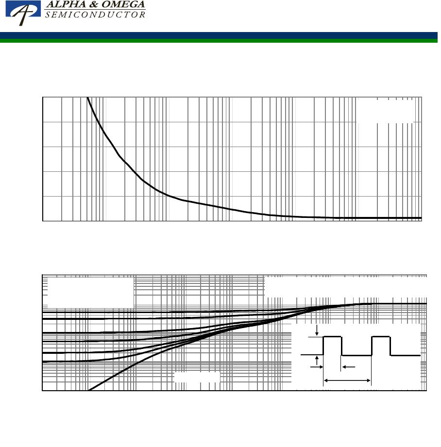
Figure 15: Normalized Maximum Transient Thermal Impedance (Note F)
Z
θ
θ
θ
θ
JC
Normalized Transient
Thermal Resistance
D=T
on
/T
T
J,PK
=T
C
+P
DM
.Z
θ
JC
.R
θ
JC
R
θ
JC
=0.45°C/W
In descending order
D=0.5, 0.3, 0.1, 0.05, 0.02, 0.01, single pulse
Single Pulse
T
on
T
P
D
Rev.1.0: September 2013
www.aosmd.com
Page 5 of 7
AOV20S60
TYPICAL ELECTRICAL AND THERMAL CHARACTERISTICS
0.001
0.01
0.1
1
10
0.0001
0.001
0.01
0.1
1
10
100
1000
10000
Pulse Width (s)
Figure 17: Normalized Maximum Transient Thermal Impedance (Note G)
Z
θ
θ
θ
θ
JC
Normalized Transient
Thermal Resistance
D=T
on
/T
T
J,PK
=T
A
+P
DM
.Z
θ
JA
.R
θ
JA
R
θ
JA
=50°C/W
In descending order
D=0.5, 0.3, 0.1, 0.05, 0.02, 0.01, single pulse
Single Pulse
0
20
40
60
80
100
0.01
0.1
1
10
100
1000
10000
Pulse Width (s)
Figure 16: Single Pulse Power Rating Junction-to-Ambient (Note G)
Power (W)
T
J(Max)
=150°C
T
A
=25°C
T
on
T
P
D
Rev.1.0: September 2013
www.aosmd.com
Page 6 of 7
P1-P3
P4-P6
P7-P7
AOV20S60
Mfr. #:
Buy AOV20S60
Manufacturer:
Description:
MOSFET N-CH 600V 18A 5DFB
Lifecycle:
New from this manufacturer.
Delivery:
DHL
FedEx
Ups
TNT
EMS
Payment:
T/T
Paypal
Visa
MoneyGram
Western
Union
Products related to this Datasheet
AOV20S60