NJM4558/4559
-
-
Ver.2013-11-05
■ TYPICAL CHARACTERISTICS
[CAUTION]
The specifications on this databook are only
given for information , without any guarantee
as regards either mistakes or omissions. The
application circuits in this databook are
described only to show representative usages
of the product and not intended for the
guarantee or permission of any right including
the industrial rights.
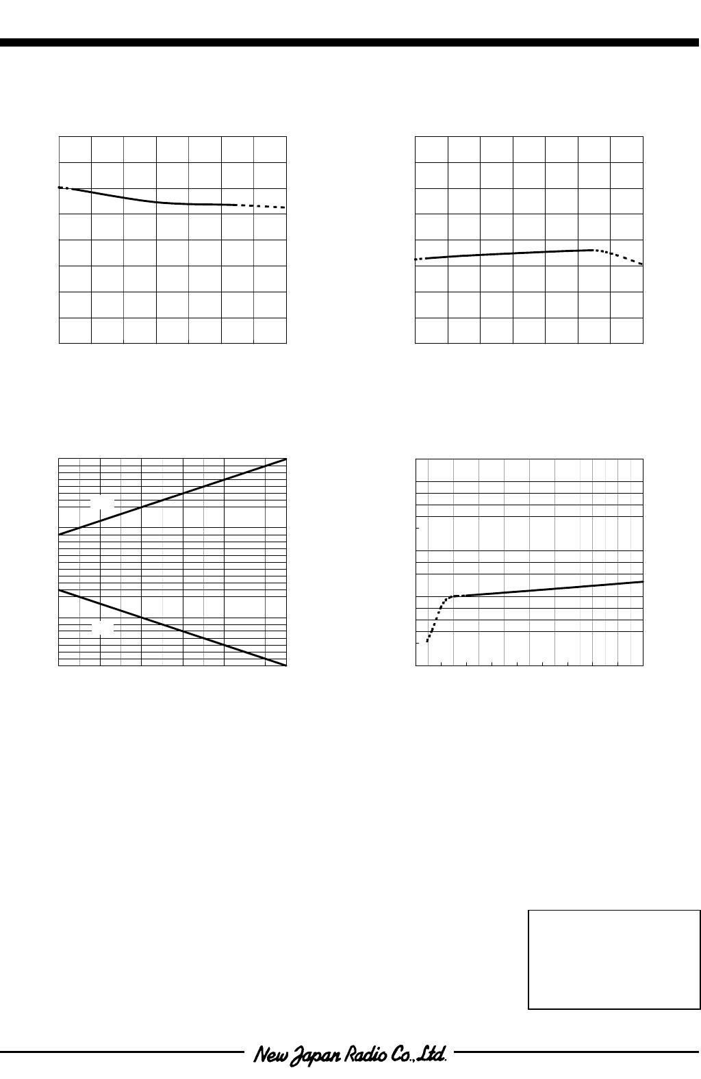
Input Offset Voltage vs. temperature
V
+
/V
-
=±15V
-2
-1.5
-1
-0.5
0
0.5
1
1.5
2
-50 -25 0 25 50 75 100 125
Ambient Temperature Ta [ºC]
Input Offset Voltage V
IO
[mV]
Input Bias Current vs. Temperature
V
+
/V
-
=±15V
5
10
15
20
25
30
35
40
45
-50 -25 0 25 50 75 100 125
Ambient Temperature Ta [ºC]
Input Bias Current I
B
[nA]
Maximum Output Voltage Swing
vs. Operating Voltage
R
L
=2kΩ, Ta=25ºC
-15
-10
-5
0
5
10
15
±6 ±8 ±10 ±12 ±14 ±16
Operating Voltage V
+
/V
-
[V]
+V
OM
-V
OM
Maximum Output Voltage Swing [V]
Operating Current vs. Operating Voltage
Ta=25ºC
0
1
2
3
4
5
6
7
8
9
0 ±2 ±4 ±6 ±8 ±10 ±12 ±14 ±16 ±18
Operating Voltage V
+
/V
-
[V]
Operating Current I
CC
[mA]