NJM4558M

NJM4558/4559
-
1
-
Ver.2013-11-05
DUAL OPERATIONAL AMPLIFIER
GENERAL DESCRIPTION PACKAGE OUTLINE
The NJM4558/4559 integrated circuit is a dual high-gain
operational amplifier internally compensated and constructed on a
single silicon chip using an advanced epitaxial process.
Combining the features of the NJM741 with the close parameter
matching and tracking of a dual device on a monolithic chip results
in unique performance characteristics. Excellent channel
separation allows the use of the dual device in single NJM741
operational amplifier applications providing density. It is especially
well suited for applications in differential-in, differential-out as well
as in potentiometric amplifiers and where gain and phase
matched channels are mandatory.
FEATURES
Operating Voltage ( ±4V~±18V )
High Voltage Gain ( 100dB typ. )
High Input Resistance ( 5M typ. )
Bipolar Technology
Package Outline DIP8, DMP8, SIP8
SOP8 JEDEC 150mil (only NJM4558),
SSOP8 (only NJM4558)
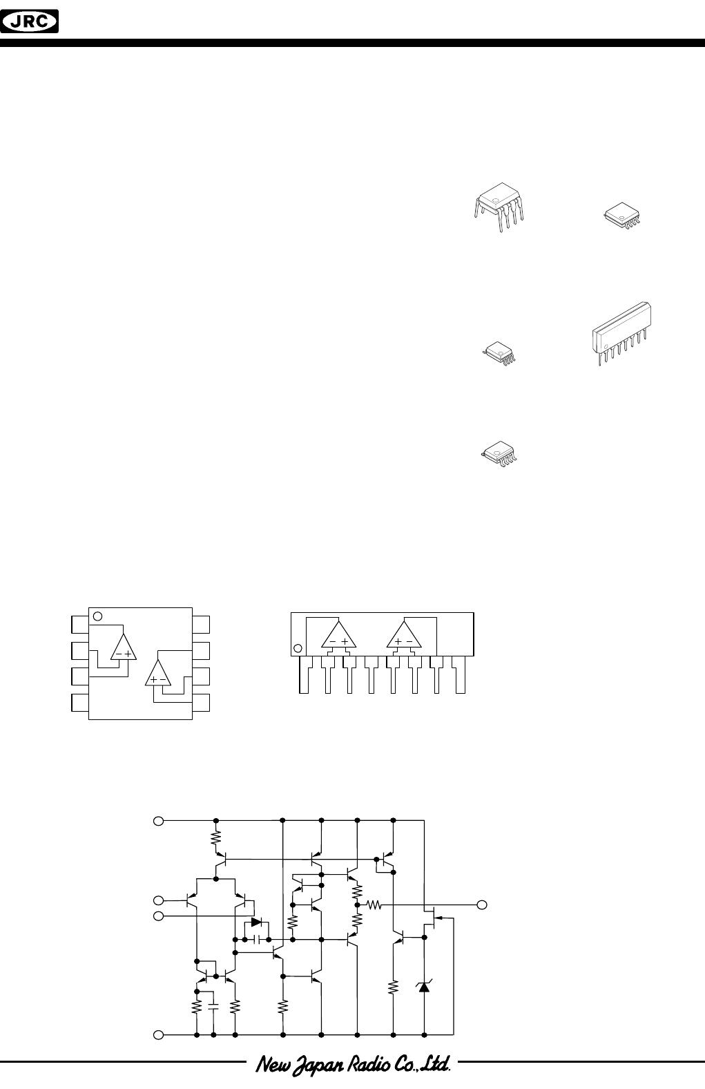
PIN CONFIGURATION
EQUIVALENT CIRCUIT ( 1/2 Shown )
NJM4558D
NJM4559D
( DIP8 )
NJM4558M
NJM4559M
( DMP8 )
NJM4558V
( SSOP8 )
NJM4558L
NJM4559L
( SIP8 )
NJM4558E
( SOP8 )
PIN FUNCTION
1. A OUTPUT
2. A - INPUT
3. A +INPUT
4. V
-
5. B +INPUT
6. B - INPUT
7. B OUTPUT
8. V
+
8
7
6
5
1
2
3
4
A
B
( Top View )
NJM4558D, NJM4558M, NJM4558E, NJM4558
V
NJM4559D, NJM4559M
A B
1 234567 8
NJM4558
L
NJM4559L
- INPUT
V
+
OUTPUT
+ INPUT
V
-
NJM4558/4559
-
2
-
Ver.2013-11-05
ABSOLUTE MAXIMUM RATINGS
( Ta=25˚C )
PARAMETER SYMBOL RATINGS UNIT
Supply Voltage V
+
/V
-
± 18 V
Differential Input Voltage V
ID
± 30 V
Input Voltage V
IC
± 15 ( note1 ) V
( DIP8 ) 500
( DMP8 ) 300
( SOP8 ) 300
( SSOP8 ) 250
Power Dissipation P
D
( SIP8 ) 800
mW
Operating Temperature Range T
opr
-40~+85 ˚C
Storage Temperature Range T
stg
-40~+125 ˚C
( note1 ) For supply voltage less than ±15V,the absolute maximum input voltage is equal to the supply voltage.
ELECTRICAL CHARACTERISTICS
( V
+
/V
-
=±15V,Ta =25˚C )
PARAMETER SYMBOL TEST CONDITION MIN. TYP. MAX. UNIT
Input Offset Voltage V
IO
R
S
10k
- 0.5 6 mV
Input Offset Current I
IO
- 5 200 nA
Input Bias Current I
B
- 25 500 nA
Input Resistance R
IN
0.3 5 - M
Large Signal Voltage Gain A
V
R
L
2k,V
O
=±10V 86 100 - dB
Maximum Output Voltage Swing 1 V
OM1
R
L
10k ± 12 ± 14 - V
Maximum Output Voltage Swing 2 V
OM2
R
L
2k ± 10 ± 13 - V
Input Common Mode Voltage Range V
ICM
± 12 14 - V
Common Mode Rejection Ratio CMR
R
S
10k
70 90 - dB
Supply Voltage Rejection Ratio SVR
R
S
10k
76.5 90 - dB
Operating Current I
CC
- 3.5 5.7 mA
Slew Rate
NJM4558 SR - 1 - V/µs
NJM4559 SR - 2 - V/µs
Equivalent Input Noise Voltage (note2) V
NI
RIAA,R
S
=2.2k,30kHz LPF - 1.4 - µVrms
Gain Bandwidth Product GB
NJM4558 3 MHz
NJM4559 6 MHz
(note2) In regard to Noise Standard, NJRC is preparing for special D Rank type products (V
NI
=1.8µV max.) except for SSOP package.
NJM4558/4559
-
3
-
Ver.2013-11-05
TYPICAL CHARACTERISTICS
Open Loop Voltage Gain vs. Frequency
V
+
/V
-
=±15V, R
L
=2k, Ta=25ºC
0
20
40
60
80
100
120
1 10 100 1k 10k 100k 1M 10M
Frequency f [Hz]
Open Loop Voltage Gain Av [dB]
NJM4558
NJM4559
Maximum Output Voltage Swing vs. Frequency
V
+
/V
-
=±15V, R
L
=2k, Ta=25ºC
0
5
10
15
20
25
30
1 10 100 1k 10k 100k 1M
Frequency f [Hz]
NJM4558
NJM4559
Maximum Output Voltage Swing V
opp
[V]
Maximum Output Voltage Swing vs.
Load Resistance
V
+
/V
-
=±15V, Ta=25ºC
12
14
16
18
20
22
24
26
28
30
100 1k 10k
Load Resistance R
L
[]
Maximum Output Voltage Swing V
opp
[V]
Operating Current vs. Temperature
V
+
/V
-
=±15V
0
1
2
3
4
5
6
7
8
9
-50 -25 0 25 50 75 100 125
Ambient Temperature Ta [ºC]
Operating Current I
cc
[mA]
Maximum Output Voltage Swing vs. Temperature
V
+
/V
-
=±15V, R
L
=10k
10
11
12
13
14
15
-50 -25 0 25 50 75 100 125
Ambient Temperature Ta [ºC]
-14
-13
-12
-11
-10
-9
+V
OM
-V
OM
-12
-13
-14
Maximum Output Voltage Swing [V]
Equivalent Input Noise Voltage vs. Frequency
V
+
/V
-
=±15V, R
S
=50, A
V
=60dB, Ta=25ºC
1
10
100
1000
1 10 100 1k
Frequency f [Hz]
Equivalent Input Noise Voltage en [nV
/
Hz]

NJM4558M

Mfr. #:
Manufacturer:
NJR (New Japan Radio)
Description:
Operational Amplifiers - Op Amps Dual High Gain
Lifecycle:
New from this manufacturer.
Delivery:
DHL FedEx Ups TNT EMS
Payment:
T/T Paypal Visa MoneyGram Western Union

Products related to this Datasheet