LT6660
9
6660fa
HYSTERESIS (ppm)
–240 –160 –80 0
NUMBER OF UNITS
8
70°C TO 25°C 0°C TO 25°C
10
12
6660 F06
6
4
80
160
–200 –120 –40 40
120
200
2
0
18
16
14
240
WORST-CASE HYSTERESIS
ON 40 UNITS
HYSTERESIS (ppm)
–600 –400 –200 0
NUMBER OF UNITS
4
85°C TO 25°C –40°C TO 25°C
5
6
6660 F07
3
2
200
400
–500 –300 –100 100
300
500
1
0
9
8
7
600
WORST-CASE HYSTERESIS
ON 34 UNITS
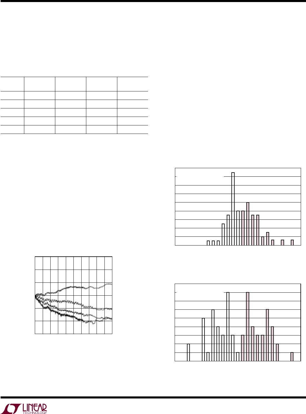
Figure 6. 0°C to 70°C Hysteresis
Figure 7. –40°C to 85°C Hysteresis
Figure 5. Typical Long-Term Drift
HOURS
–150
ppm
–50
50
150
–100
0
100
200 400 600 800
6660 F05
10001000 300 500 700 900
APPLICATIO S I FOR ATIO
W UU
U
Table 1 gives the maximum output capacitance for vari-
ous load currents and output voltages to avoid instability.
Load capacitors with low ESR (effective series resistance)
cause more ringing than capacitors with higher ESR such
as polarized aluminum or tantalum capacitors.
Table 1. Maximum Output Capacitance
VOLTAGE
OPTION I
OUT
= 100µA I
OUT
= 1mA I
OUT
= 10mA I
OUT
= 20mA
2.5V >10µF >10µF 2µF 0.68µF
3V >10µF >10µF 2µF 0.68µF
3.3V >10µF >10µF 1µF 0.68µF
5V >10µF >10µF 1µF 0.68µF
10V >10µF 1µF 0.15µF 0.1µF
Long-Term Drift
Long-term drift cannot be extrapolated from accelerated
high temperature testing. This erroneous technique
gives drift numbers that are wildly optimistic. The only
way long-term drift can be determined is to measure it
over the time interval of interest. The LT6660 long-term
drift data was taken on over 100 parts that were soldered
into PC boards similar to a “real world” application. The
boards were then placed into a constant temperature oven
with T
A
= 30°C, their outputs were scanned regularly and
measured with an 8.5 digit DVM. Figure 5 shows typical
long-term drift of the LT6660s.
Hysteresis
Hysteresis data shown in Figure 6 and Figure 7 represents
the worst-case data taken on parts from 0°C to 70°C and
from –40°C to 85°C. The output is capable of dissipat-
ing relatively high power, i.e., for the LT6660-2.5, P
D
=
17.5V • 20mA = 350mW. The thermal resistance of the
DFN package is 102°C/W and this dissipation causes a
36°C internal rise. This elevated temperature may cause
the output to shift due to thermal hysteresis. For highest
performance in precision applications, do not let the
LT6660’s junction temperature exceed 85°C.
Input Capacitance
It is recommended that a 0.1µF or larger capacitor be
added to the input pin of the LT6660. This can help with
stability when large load currents are demanded.