© Semiconductor Components Industries, LLC, 2013
December, 2013 − Rev. 14
Publication Order Number:
BD676/D
BD676G, BD676AG,
BD678G, BD678AG,
BD680G, BD680AG,
BD682G, BD682TG
Plastic Medium-Power
Silicon PNP Darlingtons
This series of plastic, medium−power silicon PNP Darlington
transistors can be used as output devices in complementary
general−purpose amplifier applications.
Features
• High DC Current Gain
• Monolithic Construction
• BD676, 676A, 678, 678A, 680, 680A, 682 are complementary
with BD675, 675A, 677, 677A, 679, 679A, 681
• BD678, 678A, 680, 680A are equivalent to MJE 700, 701, 702, 703
• These Devices are Pb−Free and are RoHS Compliant*
MAXIMUM RATINGS
Rating Symbol Value Unit
Collector-Emitter Voltage
BD676G, BD676AG
BD678G, BD678AG
BD680G, BD680AG
BD682G, BD682TG
V
CEO
45
60
80
100
Vdc
Collector-Base Voltage
BD676G, BD676AG
BD678G, BD678AG
BD680G, BD680AG
BD682G, BD682TG
V
CB
45
60
80
100
Vdc
Emitter-Base Voltage V
EB
5.0 Vdc
Collector Current I
C
4.0 Adc
Base Current I
B
0.1 Adc
Total Device Dissipation
@ T
C
= 25°C
Derate above 25°C
P
D
40
0.32
W
W/°C
Operating and Storage Junction
Temperature Range
T
J
, T
stg
−55 to +150 °C
Stresses exceeding those listed in the Maximum Ratings table may damage the
device. If any of these limits are exceeded, device functionality should not be
assumed, damage may occur and reliability may be affected.
THERMAL CHARACTERISTICS
Characteristic Symbol Max Unit
Thermal Resistance,
Junction−to−Case
R
q
JC
3.13 °C/W
*For additional information on our Pb−Free strategy and soldering details, please
download the ON Semiconductor Soldering and Mounting Techniques
Reference Manual, SOLDERRM/D.
4.0 AMP DARLINGTON
POWER TRANSISTORS
PNP SILICON
45, 60, 80, 100 VOLT, 40 WATT
http://onsemi.com
See detailed ordering and shipping information in the package
dimensions section on page 3 of this data sheet.
ORDERING INFORMATION
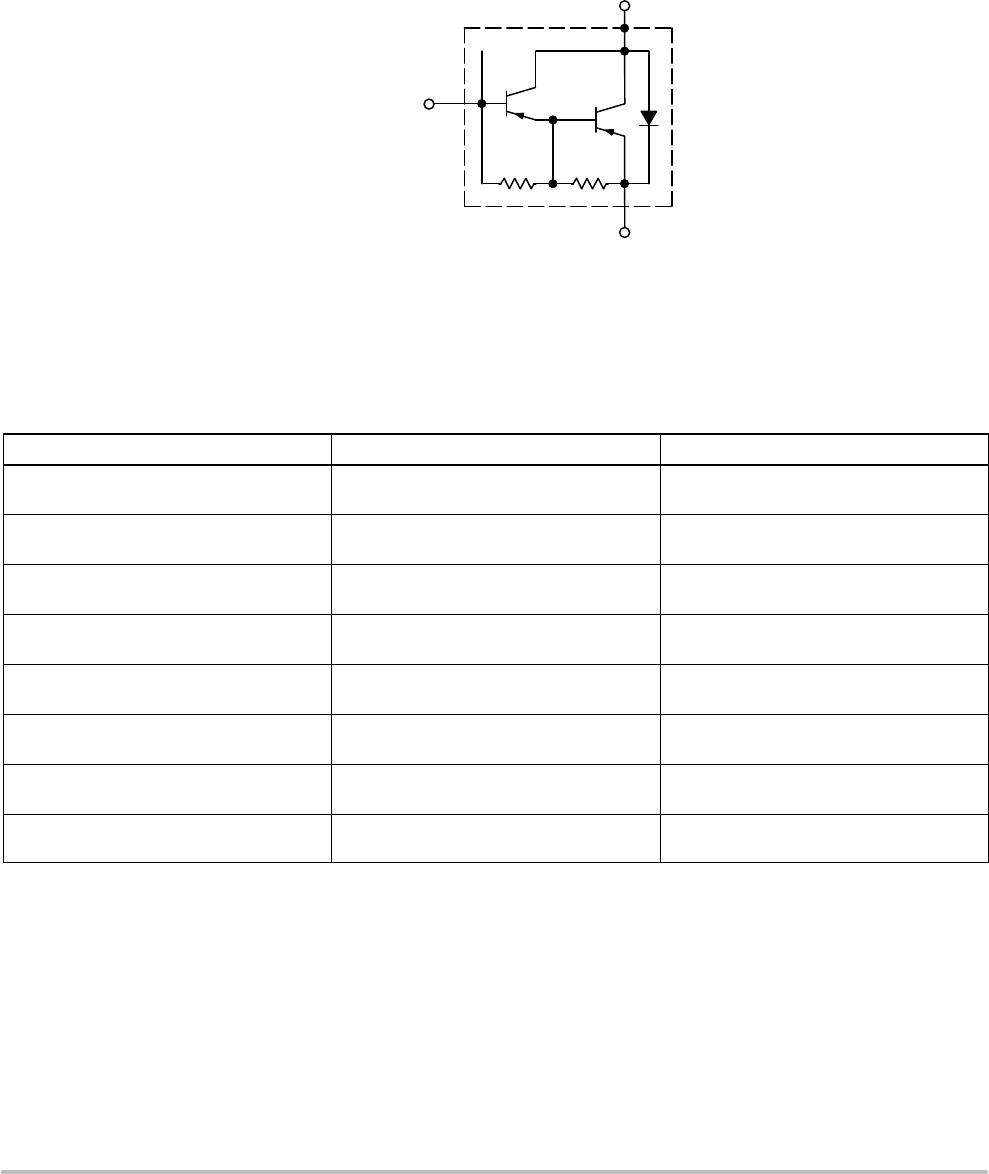
MARKING DIAGRAMS
Y = Year
WW = Work Week
BD6xx = Device Code
xx = 76, 78, 80, 82, or 82T
G = Pb−Free Package
COLLECTOR 2, 4
BASE 3
EMITTER 1
TO−225
CASE 77−09
STYLE 1
1
2
3
YWW
BD6xxG
YWW
BD6xxAG