574MLFT

DATASHEET
ZERO DELAY, LOW SKEW BUFFER ICS574
IDT™/ ICS™
ZERO DELAY, LOW SKEW BUFFER 1
ICS574 REV G 051310
Description
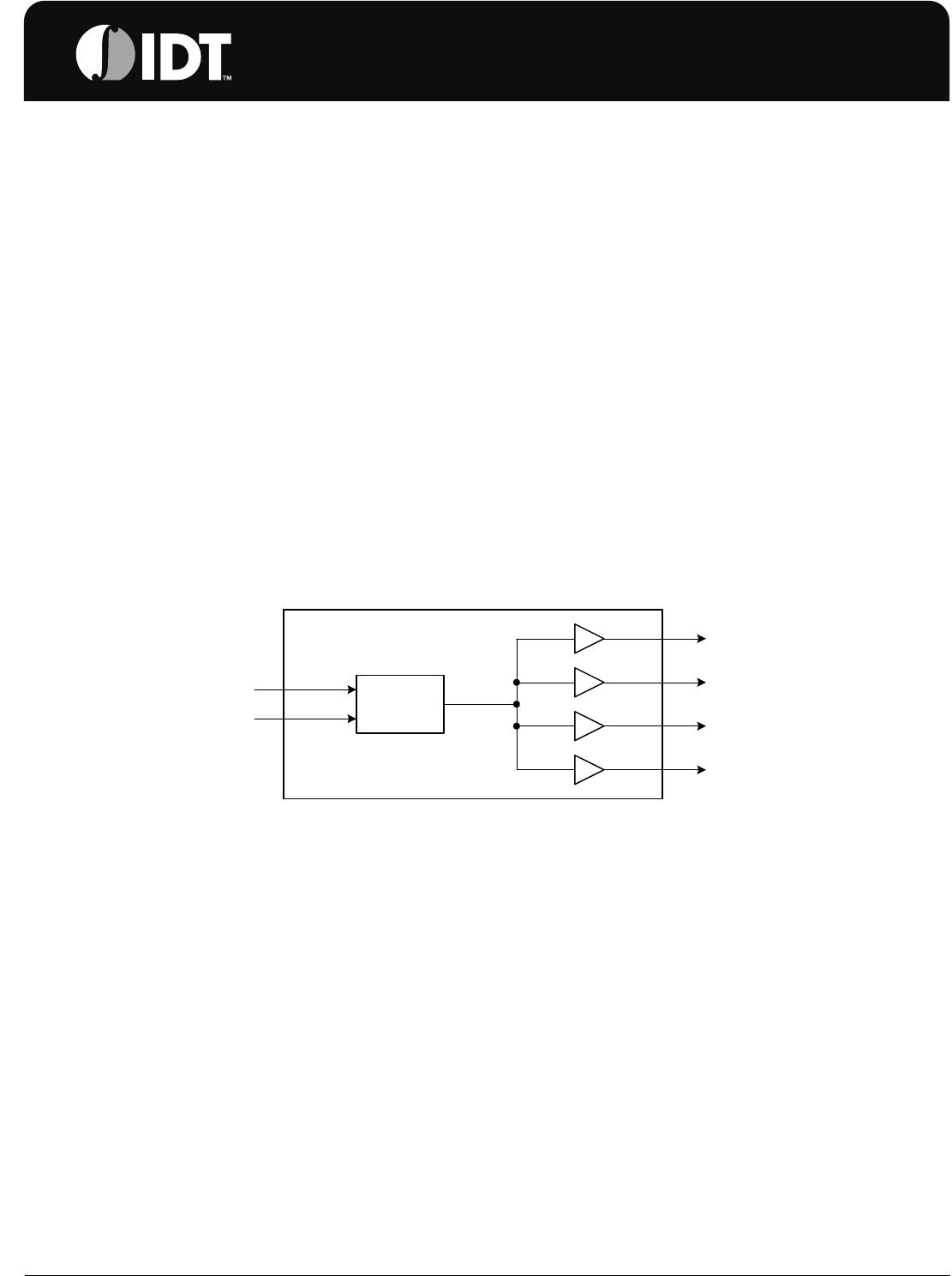
The ICS574 is a low jitter, low-skew, high performance
PLL-based zero delay buffer for high speed applications.
Based on IDT’s proprietary low jitter Phase Locked Loop
(PLL) techniques, the device provides four low skew
outputs at speeds up to 160 MHz at 3.3 V. When one of the
outputs is connected directly to FBIN, the rising edge of
each output is aligned with the rising edge of the input
clock. External delay elements connected in the feedback
loops will cause the outputs to occur before the inputs by
the amount of propagation delay of the external element.
Features
Packaged in 8 pin narrow SOIC, Pb (lead) free
Zero input-to-output delay
Four 1X outputs
Output to output skew is less than 150 ps
Output clocks up to 160 MHz at 3.3 V
External feedback path for output edge placement
Spread Smart™ technology works with spread spectrum
clock generators
Full CMOS outputs with 18 mA output drive capability at
TTL levels at 3.3 V
Advanced, low power, sub-micron CMOS process
Operating voltage from 3.0 to 5.5 V
Industrial temperature version available
Block Diagram
PLL
FBIN
CLKIN
CLK1
CLK2
CLK3
CLK4
ICS574
ZERO DELAY, LOW SKEW BUFFER ZDB
IDT™/ ICS™
ZERO DELAY, LOW SKEW BUFFER 2
ICS574 REV G 051310
Pin Assignment
Pin Descriptions
CLKIN
CLK1
CLK2
GND
CLK3
FBIN1
2
3
4
8
7
6
5
CLK4
VDD
Pin
Number
Pin
Name
Pin
Type
Pin Description
1 CLKIN Input Clock input. Connect to input clock source.
2, 3, 6, 7 CLK1:4 Output Clock Outputs (4).
4 GND Power Connect to ground.
5 VDD Power Power supply. Connect both pins to same voltage (either 3.3 V or 5 V).
8 FBIN Input Feedback input.
ICS574
ZERO DELAY, LOW SKEW BUFFER ZDB
IDT™/ ICS™
ZERO DELAY, LOW SKEW BUFFER 3
ICS574 REV G 051310
External Components
The ICS574 requires a minimum number of external components for proper operation. Decoupling capacitors of
0.1µF should be connected between VDD and GND on pins 4 and 5, as close to the device as possible. A series
termination resistor of 33 may be used close to the pin for each clock output to reduce reflections.
Absolute Maximum Ratings
Stresses above the ratings listed below can cause permanent damage to the ICS574. These ratings, which are
standard values for IDT commercially rated parts, are stress ratings only. Functional operation of the device at these
or any other conditions above those indicated in the operational sections of the specifications is not implied.
Exposure to absolute maximum rating conditions for extended periods can affect product reliability. Electrical
parameters are guaranteed only over the recommended operating temperature range.
Item Rating
Supply Voltage, VDD (referenced to ground) -0.5 V to 7 V
All Inputs and Outputs -0.5 V to VDD+0.5 V
Electrostatic Discharge (MIl-STD-883) 2000 V (minimum)
Ambient Operating Temperature -40° C to +85° C
Soldering Temperature (10 seconds max.) 260° C
Junction Temperature 150° C
Storage Temperature -65 to +150° C

574MLFT

Mfr. #:
Manufacturer:
IDT
Description:
Clock Buffer ZERO DELAY, LOW SKEW BUFFER
Lifecycle:
New from this manufacturer.
Delivery:
DHL FedEx Ups TNT EMS
Payment:
T/T Paypal Visa MoneyGram Western Union

Products related to this Datasheet