BDX53CG

© Semiconductor Components Industries, LLC, 2014
November, 2014 − Rev. 15
1 Publication Order Number:
BDX53B/D
BDX53B, BDX53C (NPN),
BDX54B, BDX54C (PNP)
Plastic Medium-Power
Complementary Silicon
Transistors
These devices are designed for general−purpose amplifier and
low−speed switching applications.
Features
High DC Current Gain −
h
FE
= 2500 (Typ) @ I
C
= 4.0 Adc
Collector Emitter Sustaining Voltage − @ 100 mAdc
V
CEO(sus)
= 80 Vdc (Min) − BDX53B, 54B
V
CEO(sus)
= 100 Vdc (Min) − BDX53C, 54C
Low Collector−Emitter Saturation Voltage −
V
CE(sat)
= 2.0 Vdc (Max) @ I
C
= 3.0 Adc
V
CE(sat)
= 4.0 Vdc (Max) @ I
C
= 5.0 Adc
Monolithic Construction with Built−In Base−Emitter Shunt Resistors
These Devices are Pb−Free and are RoHS Compliant*
MAXIMUM RATINGS
Rating Symbol Value Unit
Collector−Emitter Voltage
BDX53B, BDX54B
BDX53C, BDX54C
V
CEO
80
100
Vdc
Collector−Base Voltage
BDX53B, BDX54B
BDX53C, BDX54C
V
CB
80
100
Vdc
Emitter−Base Voltage V
EB
5.0 Vdc
Collector Current − Continuous
− Peak
I
C
8.0
12
Adc
Base Current I
B
0.2 Adc
Total Device Dissipation @ T
C
= 25°C
Derate above 25°C
P
D
65
0.48
W
W/°C
Operating and Storage Junction
Temperature Range
T
J
, T
stg
65 to +150 °C
Stresses exceeding those listed in the Maximum Ratings table may damage the
device. If any of these limits are exceeded, device functionality should not be
assumed, damage may occur and reliability may be affected.
THERMAL CHARACTERISTICS
Characteristic Symbol Max Unit
Thermal Resistance, Junction−to−Ambient
R
q
JA
70 °C/W
Thermal Resistance, Junction−to−Case
R
q
JC
1.92 °C/W
*For additional information on our Pb−Free strategy and soldering details, please
download the ON Semiconductor Soldering and Mounting Techniques
Reference Manual, SOLDERRM/D.
DARLINGTON
8 AMPERE
COMPLEMENTARY SILICON
POWER TRANSISTORS
80100 VOLTS, 65 WATTS
TO−220
CASE 221A
STYLE 1
1
2
3
4
MARKING DIAGRAM
& PIN ASSIGNMENT
1
Base
3
Emitter
4
Collector
2
Collector
www.onsemi.com
BDX5xy = Device Code
x = 3 or 4
y = B or C
A = Assembly Location
Y = Year
WW = Work Week
G = Pb−Free Package
BDX5xyG
AY WW
See detailed ordering and shipping information in the package
dimensions section on page 6 of this data sheet.
ORDERING INFORMATION
BDX53B, BDX53C (NPN), BDX54B, BDX54C (PNP)
www.onsemi.com
2
80
40
20
0
20 40 80 100 120 160
Figure 1. Power Derating
T, TEMPERATURE (°C)
P
D
, POWER DISSIPATION (WATTS)
60
T
A
T
C
4.0
2.0
1.0
3.0
0 60 140
T
A
T
C
ELECTRICAL CHARACTERISTICS (T
C
= 25°C unless otherwise noted)
Characteristic
Symbol Min Max Unit
OFF CHARACTERISTICS
Collector−Emitter Sustaining Voltage (Note 1)
(I
C
= 100 mAdc, I
B
= 0) BDX53B, BDX54B
BDX53C, BDX54C
V
CEO(sus)
80
100
Vdc
Collector Cutoff Current
(V
CE
= 40 Vdc, I
B
= 0) BDX53B, BDX54B
(V
CE
= 50 Vdc, I
B
= 0) BDX53C, BDX54C
I
CEO
0.5
0.5
mAdc
Collector Cutoff Current
(V
CB
= 80 Vdc, I
E
= 0) BDX53B, BDX54B
(V
CB
= 100 Vdc, I
E
= 0) BDX53C, BDX54C
I
CBO
0.2
0.2
mAdc
ON CHARACTERISTICS (Note 1)
DC Current Gain
(I
C
= 3.0 Adc, V
CE
= 3.0 Vdc)
h
FE
750
Collector−Emitter Saturation Voltage
(I
C
= 3.0 Adc, I
B
= 12 mAdc)
V
CE(sat)
2.0
4.0
Vdc
Base−Emitter Saturation Voltage
(I
C
= 3.0 Adc, I
C
= 12 mA)
V
BE(sat)
2.5 Vdc
DYNAMIC CHARACTERISTICS
Small−Signal Current Gain
(I
C
= 3.0 Adc, V
CE
= 4.0 Vdc, f = 1.0 MHz)
h
fe
4.0
Output Capacitance
(V
CB
= 10 Vdc, I
E
= 0, f = 0.1 MHz) BDX53B, 53C
BDX54B, 54C
C
ob
300
200
pF
Product parametric performance is indicated in the Electrical Characteristics for the listed test conditions, unless otherwise noted. Product
performance may not be indicated by the Electrical Characteristics if operated under different conditions.
1. Pulse Test: Pulse Width 300 ms, Duty Cycle 2%.
BDX53B, BDX53C (NPN), BDX54B, BDX54C (PNP)
www.onsemi.com
3
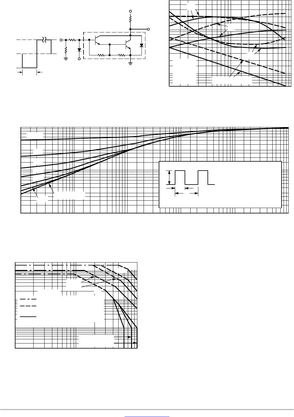
Figure 2. Switching Time Test Circuit
5.0
0.1
Figure 3. Switching Times
I
C
, COLLECTOR CURRENT (AMP)
t, TIME (s)μ
3.0
0.7
0.5
0.3
0.2
0.05
0.2 0.3 0.7 3.0 10
t
d
@ V
BE(off)
= 0 V
V
CC
= 30 V
I
C
/I
B
= 250
I
B1
= I
B2
T
J
= 25°C
t
f
0.07
1.0 5.0
t
s
t
r
0.1
1.0
2.0
0.5 2.0 7.0
0
V
CC
- 30 V
SCOPE
TUT
+ 4.0 V
t
r
, t
f
v 10 ns
DUTY CYCLE = 1.0%
R
C
D
1
MUST BE FAST RECOVERY TYPES, e.g.:
1N5825 USED ABOVE I
B
[ 100 mA
MSD6100 USED BELOW I
B
[ 100 mA
25 ms
D
1
51
R
B
AND R
C
VARIED TO OBTAIN DESIRED CURRENT LEVELS
V
2
APPROX
+ 8.0 V
V
1
APPROX
-12 V
[ 8.0 k [ 120
for t
d
and t
r
, D
1
is disconnected
and V
2
= 0
For NPN test circuit reverse all polarities
R
B
Figure 4. Thermal Response
t, TIME OR PULSE WIDTH (ms)
1.0
0.01
0.01
0.7
0.5
0.3
0.2
0.1
0.07
0.05
0.03
0.02
0.02
r(t) EFFECTIVE TRANSIENT
THERMAL RESISTANCE (NORMALIZED)
0.05 0.1 0.2 0.5 1.0 2.0 5.0 10 20 50 100 200 1000500
R
q
JC
(t) = r(t) R
q
JC
R
q
JC
= 1.92°C/W
D CURVES APPLY FOR POWER
PULSE TRAIN SHOWN
READ TIME AT t
1
T
J(pk)
- T
C
= P
(pk)
R
q
JC
(t)
P
(pk)
t
1
t
2
DUTY CYCLE, D = t
1
/t
2
D = 0.5
SINGLE PULSE
0.2
0.05
0.1
0.02
0.01
SINGLE
PULSE
0.03 0.3 3.0 30 300
BONDING WIRE LIMITED
THERMALLY LIMITED @ T
C
= 25°C
(SINGLE PULSE)
SECOND BREAKDOWN LIMITED
1.0
Figure 5. Active−Region Safe Operating Area
20
2.0
0.05
10 20 100
T
J
= 150°C
0.2
5.0
0.5
I
C
, COLLECTOR CURRENT (AMP)
V
CE
, COLLECTOR-EMITTER VOLTAGE (VOLTS)
10
30 70
1.0
0.1
dc
2.0 503.0 5.0 7.0
5.0 ms
1.0 ms
100 ms
BDX53B, BDX54B
BDX53C, BDX54C
CURVES APPLY BELOW RATED V
CEO
0.02
500 ms
There are two limitations on the power handling ability of
a transistor average junction temperature and second
breakdown. Safe operating area curves indicate I
C
−V
CE
limits of the transistor that must be observed for reliable
operation, i.e., the transistor must not be subjected to greater
dissipation than the curves indicate.
The data of Figure 5 is based on T
J(pk)
= 150°C; T
C
is
variable depending on conditions. Second breakdown pulse
limits are valid for duty cycles to 10% provided
T
J(pk)
t 150°C. T
J(pk)
may be calculated from the data in
Figure 4. At high case temperatures, thermal limitations will
reduce the power that can be handled to values less than the
limitations imposed by second breakdown.

BDX53CG

Mfr. #:
Manufacturer:
ON Semiconductor
Description:
Darlington Transistors 8A 100V Bipolar Power NPN
Lifecycle:
New from this manufacturer.
Delivery:
DHL FedEx Ups TNT EMS
Payment:
T/T Paypal Visa MoneyGram Western Union

Products related to this Datasheet