PCA9517A All information provided in this document is subject to legal disclaimers. © NXP Semiconductors N.V. 2016. All rights reserved.
Product data sheet Rev. 4.1 — 24 May 2016 11 of 22
NXP Semiconductors
PCA9517A
Level translating I
2
C-bus repeater
[1] LOW-level supply voltage.
[2] V
IL
specification is for the first LOW level seen by the SDAB/SCLB lines. V
ILc
is for the second and subsequent LOW levels seen by the
SDAB/SCLB lines.
[3] V
IL
for port A with envelope noise must be below 0.3V
CC(A)
for stable performance.
10. Dynamic characteristics
[1] Times are specified with loads of 1.35 k pull-up resistance and 57 pF load capacitance on port B, and 167 pull-up resistance and
57 pF load capacitance on port A. Different load resistance and capacitance will alter the RC time constant, thereby changing the
propagation delay and transition times.
[2] Pull-up voltages are V
CC(A)
on port A and V
CC(B)
on port B.
[3] Typical values were measured with V
CC(A)
= 3.3 V at T
amb
=25C, unless otherwise noted.
[4] The t
PLH
delay data from port B to port A is measured at 0.5 V on port B to 0.5V
CC(A)
on port A when V
CC(A)
is less than 2 V, and 1.5 V
on port A if V
CC(A)
is greater than 2 V.
[5] Typical value measured with V
CC(A)
=2.7V at T
amb
=25C.
[6] The proportional delay data from port A to port B is measured at 0.3V
CC(A)
on port A to 1.5 V on port B.
[7] The enable pin, EN, should only change state when the global bus and the repeater port are in an idle state.
Enable
V
IL
LOW-level input voltage 0.5 - +0.3V
CC(B)
V
V
IH
HIGH-level input voltage 0.7V
CC(B)
-5.5 V
I
IL(EN)
LOW-level input current on
pin EN
V
I
= 0.2 V, EN; V
CC
=3.6V - 10 30 A
I
LI
input leakage current 1-+1 A
C
i
input capacitance V
I
=3.0V or 0V - 6 7 pF
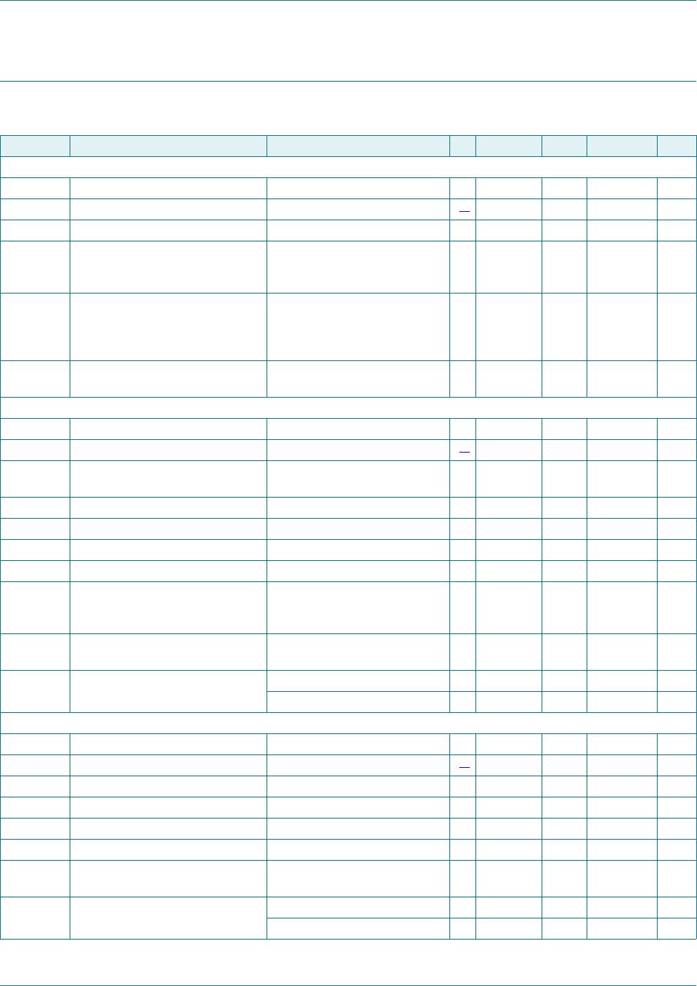
Table 5. Static characteristics
…continued
V
CC
= 2.7 V to 5.5 V; GND = 0 V; T
amb
=
40
Cto+85
C; unless otherwise specified.
Symbol Parameter Conditions Min Typ Max Unit
Table 6. Dynamic characteristics
V
CC
= 2.7 V to 5.5 V; GND = 0 V; T
amb
=
40
Cto+85
C; unless otherwise specified.
[1][2]
Symbol Parameter Conditions Min Typ
[3]
Max Unit
t
PLH
LOW to HIGH propagation delay port B to port A; Figure 13
[4]
100 170 250 ns
t
PHL
HIGH to LOW propagation delay port B to port A; Figure 11
V
CC(A)
2.7 V
[5]
30 80 110 ns
V
CC(A)
3V 10 66 300 ns
t
TLH
LOW to HIGH output transition time port A; Figure 11 10 20 30 ns
t
THL
HIGH to LOW output transition time port A; Figure 11
V
CC(A)
2.7 V
[5]
177105ns
V
CC(A)
3V 20 70 175 ns
t
PLH
LOW to HIGH propagation delay port A to port B; Figure 12
[6]
25 53 110 ns
t
PHL
HIGH to LOW propagation delay port A to port B; Figure 12
[6]
60 79 230 ns
t
TLH
LOW to HIGH output transition time port B; Figure 12 120 140 170 ns
t
THL
HIGH to LOW output transition time port B; Figure 12 30 48 90 ns
t
su
set-up time EN HIGH before START condition
[7]
100--ns
t
h
hold time EN HIGH after STOP condition
[7]
100--ns