LTC2908
4
2908fd
TYPICAL PERFORMANCE CHARACTERISTICS
SYMBOL PARAMETER CONDITIONS MIN TYP MAX UNITS
t
RST
Reset Time-Out Period
l
160 200 260 ms
t
UV
V
X
Undervoltage Detect to RST V
X
Less Than Reset Threshold V
RTX
by
More Than 1%
250 μs
V
OH
Output Voltage High RST (Note 5) I
RST
= –1μA, V
CC
= 5V (LTC2908-A1)
I
RST
= –1μA, V
CC
= 3.3V (LTC2908-B1)
I
RST
= –1μA, V
CC
= 2.5V (LTC2908-C1)
l
l
l
V
CC
– 1.5
V
CC
– 1.0
V
CC
– 1.0
V
V
V
V
OL
Output Voltage Low RST V
CC
= 0.5V, I
RST
= 5μA
V
CC
= 1.0V, I
RST
= 100μA
V
CC
= 3.0V, I
RST
= 2500μA
l
l
l
0.01
0.01
0.10
0.15
0.15
0.30
V
V
V
ELECTRICAL CHARACTERISTICS
The l denotes specifi cations which apply over the full operating temperature range, otherwise specifi cations are T
A
= 25°C. V
CC
= 5V
for the LT2908-A1, V
CC
= 3.3V for the LTC2908-B1 or V
CC
= 2.5V for the LTC2908-C1, unless otherwise noted. (Notes 2, 3)
Note 1: Stresses beyond those listed under Absolute Maximum Ratings
may cause permanent damage to the device. Exposure to any Absolute
Maximum Rating condition for extended periods may affect device
reliabilty and lifetime.
Note 2: The greater of V1, V2 is the internal supply voltage (V
CC
) for the
LTC2908-A1 and the LTC2908-B1. V1 is the internal supply voltage (V
CC
)
for the LTC2908-C1.
Note 3: All currents into pins are positive; all voltages are referenced to
GND unless otherwise noted.
Note 4: Under typical operating conditions, most of the quiescent cur-
rent is drawn from the V1 input. When V2 exceeds V1, V2 supplies most
of the quiescent current.
Note 5: The output pin RST has an internal pull-up to V
CC
of typically
6μA. However, an external pull-up resistor may be used when a faster
rise time is required or for V
OH
voltages greater than V
CC
.
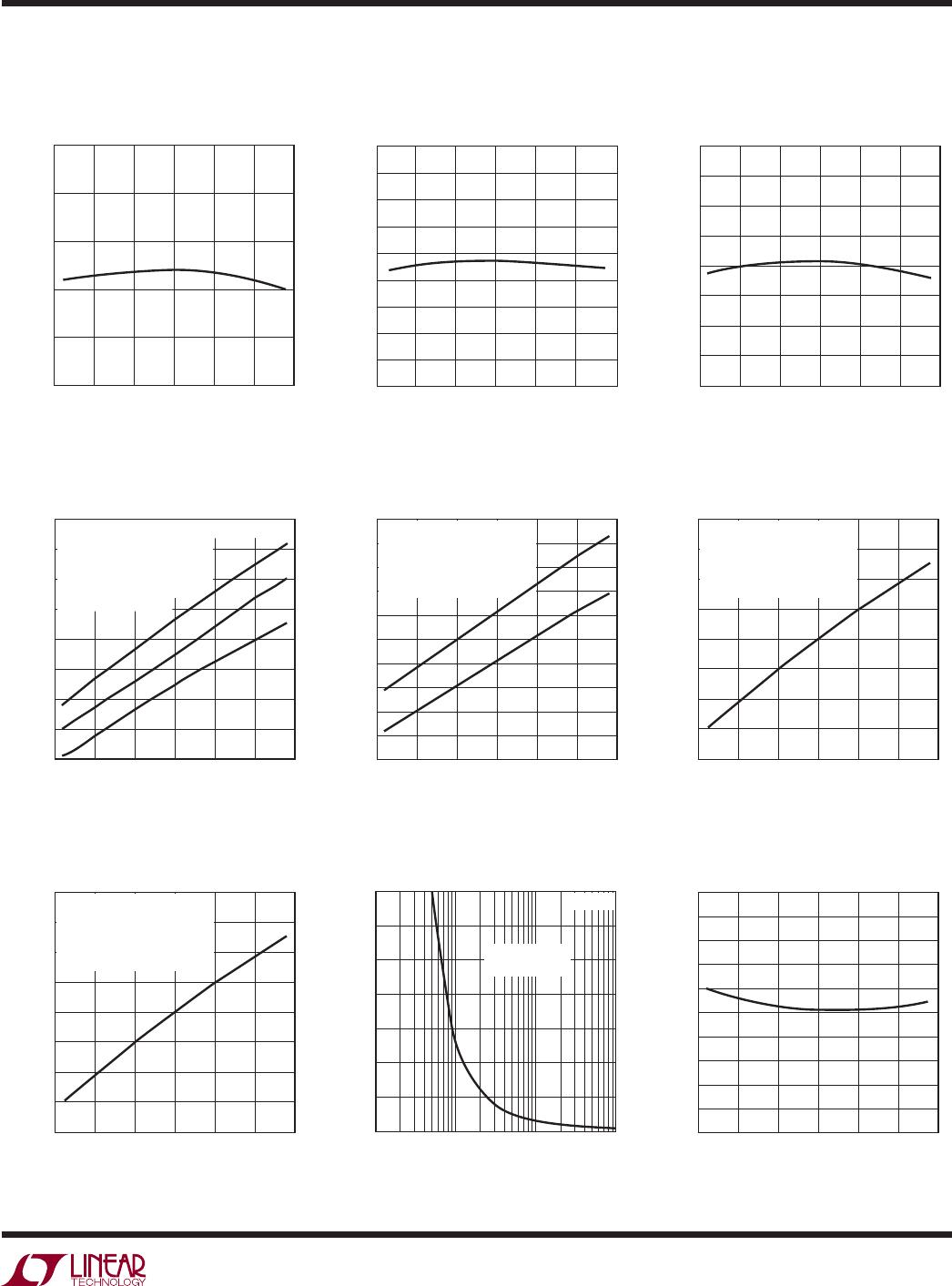
TEMPERATURE (°C)
–50
4.750
4.725
4.700
4.675
4.650
4.625
4.600
25 75
2908 G01
–25 0
50 100
THRESHOLD VOLTAGE, V
RT50
(V)
TEMPERATURE (°C)
–50
3.135
3.115
3.095
3.075
3.055
3.035
25 75
2908 G02
–25 0
50 100
THRESHOLD VOLTAGE, V
RT33
(V)
TEMPERATURE (°C)
–50
2.375
2.360
2.345
2.330
2.315
2.300
25 75
2908 G03
–25 0
50 100
THRESHOLD VOLTAGE, V
RT25
(V)
Specifi cations are at T
A
= 25°C unless otherwise noted.
5V Threshold Voltage
vs Temperature
3.3V Threshold Voltage
vs Temperature
2.5V Threshold Voltage
vs Temperature