MAX7462USA+

General Description
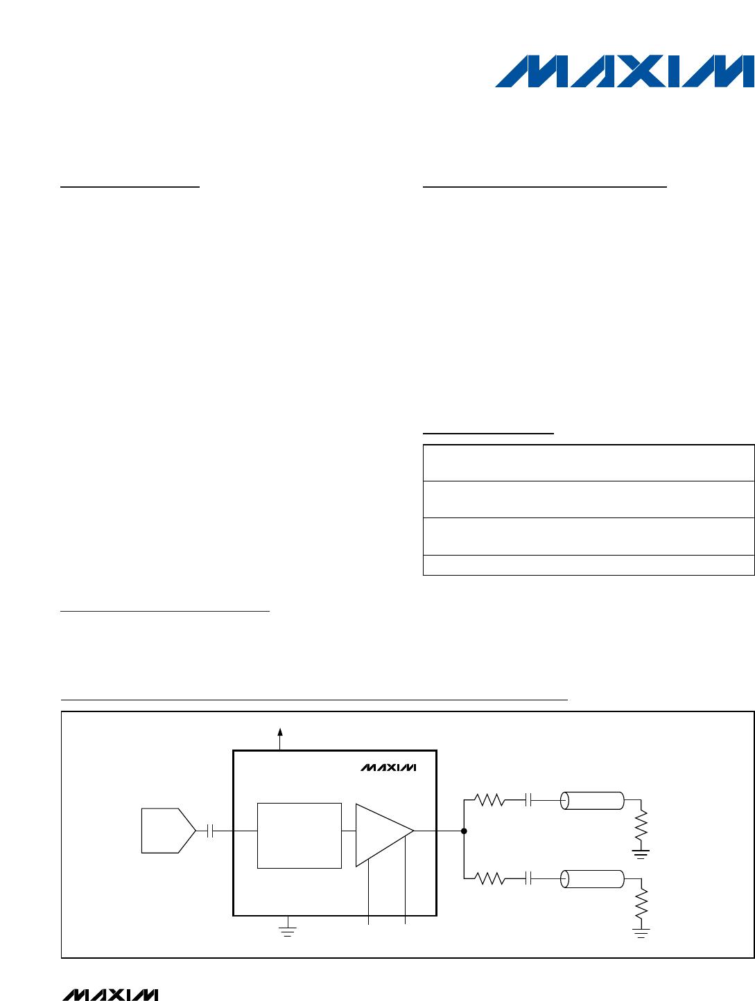
The MAX7462/MAX7463 single-channel, standard-defini-
tion, integrated video reconstruction filters and buffers
are ideal for anti-aliasing and digital-to-analog smoothing
video applications or wherever analog video is recon-
structed from digital data (such as cable/satellite/terres-
trial set-top boxes and DVRs).
The MAX7462 includes a disable function, which
places the output in a high-impedance state allowing
multiplexing of multiple output signals. It also has an
external gain control that sets the output buffer gain to
either +6dB or +9.5dB. The higher gain setting allows a
lower DAC output signal than the standard 1V
P-P
sig-
nal. The MAX7463 output buffer has a fixed gain of
+6dB.
The MAX7462/MAX7463 operate from a single +5V
supply and have a flat passband out to 5MHz with a
stopband attenuation of -43dB (typ) at 27MHz.
These devices can drive two standard 150 AC-cou-
pled or DC-coupled video loads. The output black level
of the MAX7462/MAX7463 is less than 1V for DC-cou-
pled outputs.
The MAX7462 is available in an 8-pin µMAX
®
package
and an 8-pin SO package. The MAX7463 is available in
an 8-pin SO package. All devices are specified over
the 0°C to +85°C temperature range.
Applications
Cable/Satellite/Terrestrial Set-Top Boxes
DVRs
Hard-Disk Recorders
Features
Standard-Definition CVBS Video Reconstruction
Filters and Buffers
Passband: -0.05dB at 5MHz
Stopband: -43dB at 27MHz
Selectable Gain: +6dB and +9.5dB (MAX7462)
Output Disable (MAX7462)
Drives 2V
P-P
into Two 150 Video Loads
Output Black Level < 1V for DC-Coupled Output
Very Small µMAX and SO Packages
MAX7462/MAX7463
Single-Channel Video Reconstruction Filters
and Buffers
________________________________________________________________ Maxim Integrated Products 1
19-3790; Rev 1; 9/05
For pricing, delivery, and ordering information, please contact Maxim/Dallas Direct! at
1-888-629-4642, or visit Maxim’s website at www.maxim-ic.com.
Ordering Information
PART
PIN-
PACKAGE
BUFFER GAIN
(dB)
OUTPUT
DISABLE
MAX7462UUA* 8 µMAX
+6/+9.5
selectable
Yes
MAX7462USA 8 SO
+6/+9.5
selectable
Yes
MAX7463USA 8 SO +6 fixed No
Note: All parts are specified over the 0°C to +85°C temperature
range.
*Future product—contact factory for availability.
µMAX is a registered trademark of Maxim Integrated Products, Inc.
Pin Configurations appear at end of data sheet.
75
75
220µF
220µF
*
*
Z
O
= 75
Z
O
= 75
75
75
OUT
+6dB/+9.5dB
GAIN
DISABLE
GND
LOWPASS
FILTER
V
CC
+5V
DAC
IN
0.1µF
MAX7462
*OPTIONAL
Functional Diagram
MAX7462/MAX7463
Single-Channel Video Reconstruction Filters
and Buffers
2 _______________________________________________________________________________________
ABSOLUTE MAXIMUM RATINGS
Stresses beyond those listed under “Absolute Maximum Ratings” may cause permanent damage to the device. These are stress ratings only, and functional
operation of the device at these or any other conditions beyond those indicated in the operational sections of the specifications is not implied. Exposure to
absolute maximum rating conditions for extended periods may affect device reliability.
V
CC
to GND ........................................................................+6.0V
All Other Pins to GND ...-0.3V to the lower of (V
CC
+ 0.3V) and +6V
Maximum Current into Any Pin Except V
CC
and GND .....±50mA
Continuous Power Dissipation (T
A
= +70°C)
8-Pin µMAX (derate 4.5mW/°C above +70°C) …...... 362mW
8-Pin SO (derate 5.9mW/°C above +70°C) .......... 470.6mW
Operating Temperature Range...............................0°C to +85°C
Storage Temperature Range .............................-65°C to +150°C
Lead Temperature (soldering, 10s) .................................+300°C
ELECTRICAL CHARACTERISTICS
(V
CC
= +5V ±5%, C
L
= 0 to 20pF, R
L
= 75, C
IN
= 0.1µF, gain = +6dB, DISABLE = V
CC
(MAX7462), T
A
=T
MIN
to T
MAX
, unless other-
wise noted. Typical values are at V
CC
= +5V, and T
A
= +25°C.)
PARAMETER CONDITIONS MIN TYP MAX UNITS
Passband Response f = 100kHz to 5MHz, relative to 100kHz -0.65 -0.05 +0.65 dB
Stopband Attenuation f 27MHz 39 43 dB
Output Dynamic Swing Gain = GND (MAX7462) 2.0 2.4 V
P-P
Output Sync Tip Clamp Level After termination (Note 1) 0.30 0.45 0.55 V
Group Delay Deviation f = 100kHz to 4.2MHz 11 ns
Differential Gain Five-step modulated staircase 0.15 %
Differential Phase Five-step modulated staircase 0.15 Degrees
Signal-to-Noise Ratio Output signal (2V
P-P
) to RMS noise (100Hz to 5MHz) 75 dB
Low-Frequency Gain Accuracy f =100kHz, relative to a gain of +6dB -3 +3 %
Line Time Distortion 18µs, 100 IRE bar 0.1 %
Field Time Distortion 130 lines, 18µs, 100 IRE bar 0.1 %
Power-Supply Rejection Ratio V
IN
= 100mV
P-P
, f = 100kHz 35 dB
Supply Current No load 25 35 mA
Note 1: Measured after 75back-match resistor. Assume a 75 termination resistor.
MAX7462/MAX7463
Single-Channel Video Reconstruction Filters
and Buffers
_______________________________________________________________________________________ 3
AMPLITUDE vs. FREQUENCY
MAX7462/63 toc01
FREQUENCY (MHz)
AMPLITUDE (dB)
101
-60
-40
-20
0
-80
0.1 100
NORMALIZED TO 0dB
PASSBAND AMPLITUDE
vs. FREQUENCY
MAX7462/63 toc02
FREQUENCY (MHz)
AMPLITUDE (dB)
1
-1.5
-1.0
-0.5
0
0.5
1.0
1.5
2.0
-2.0
0.1 10
NORMALIZED TO 0dB
PHASE RESPONSE
vs. FREQUENCY
MAX7462/63 toc03
FREQUENCY (MHz)
PHASE (DEGREES)
1
-150
-100
-50
0
50
100
150
200
-200
0.1 10
GROUP DELAY vs. FREQUENCY
MAX7462/63 toc04
FREQUENCY (MHz)
GROUP DELAY (ns)
1
60
70
80
90
100
50
0.1 10
200ns/div
2T RESPONSE
OUT
250mV/div
MAX7462/63 toc05
IN
250mV/div
200ns/div
MODULATED 12.5T RESPONSE
OUT
250mV/div
MAX7462/63 toc06
IN
250mV/div
Typical Operating Characteristics
(V
CC
= +5V ±5%, C
L
= 0 to 20pF, R
L
= 75, C
IN
= 0.1µF, gain = +6dB, DISABLE = V
CC
(MAX7462), T
A
=T
MIN
to T
MAX
, unless other-
wise noted. Typical values are at V
CC
= +5V, and T
A
= +25°C.)

MAX7462USA+

Mfr. #:
Manufacturer:
Maxim Integrated
Description:
Active Filters Video Reconstruction Filtr
Lifecycle:
New from this manufacturer.
Delivery:
DHL FedEx Ups TNT EMS
Payment:
T/T Paypal Visa MoneyGram Western Union