ALM-31222
1.7-2.7GHz
1-Watt High Linearity Amplier
Data Sheet
Description
Avago Technologies’ ALM-31222 is a high linearity 1 Watt
PA with good OIP3 performance and exceptionally good
PAE at 1dB gain compression point, achieved through the
use of Avago Technologies proprietary 0.25um GaAs En-
hancement-mode pHEMT process.
All matching components are fully integrated within the
module. This makes the ALM-31222 extremely easy to use.
The adjustable temperature-compensated internal bias
circuit allows the device to be operated at either class A or
class AB operation.
The ALM-31222 is housed inside a miniature 5.0 x 6.0 x 1.1
mm
3
22-lead multiple-chips-on-board (MCOB) module
package.
Component Image
5.0 x 6.0 x 1.1 mm
3
22-lead MCOB
Features
Fully matched, input and output
High linearity and P1dB
Unconditionally stable across load condition
Built-in adjustable temperature-compensated internal
bias circuitry
GaAs E-pHEMT Technology
[1]
5V supply
Excellent uniformity in product specications
Tape-and-Reel packaging option available
MSL-3 and Lead-free
High MTTF for base station application
Specications
2GHz; 5V, 415mA (typical)
14.9 dB Gain
47.9 dBm Output IP3
31.5 dBm Output Power at 1dB gain compression
52.6% PAE at P1dB
2.7 dB Noise Figure
Applications
Class A driver amplier for GSM/PCS/W-CDMA/WiMAX
Base Stations.
General purpose gain block.
Note:
1. Enhancement mode technology employs positive gate voltage,
thereby eliminating the need of negative gate voltage associated
with conventional depletion mode devices.
Notes:
Package marking provides orientation and identication
“31222” = Device Part Number
“WWYY” = Work week and Year of manufacture
“XXXX” = Last 4 digit of Lot number
31222
WWYY
XXXX
1
2
3
4
5
6
7
89
10
1112
13
14
15
16
17
18
19 21
20
22
GND
GND
VDD1
GND
VCTRL
GND
GND
GND
GND
VDD2
GND
NC
GND
GND
GND
RF_OUT
GND
GND
GND
GND
GND
NC
GND
GND
RF_IN
GND
Top View
Bottom View
Attention: Observe precautions for
handling electrostatic sensitive devices.
ESD Machine Model = 200 V
ESD Human Body Model = 700 V
Refer to Avago Application Note A004R:
Electrostatic Discharge, Damage and Control.
2
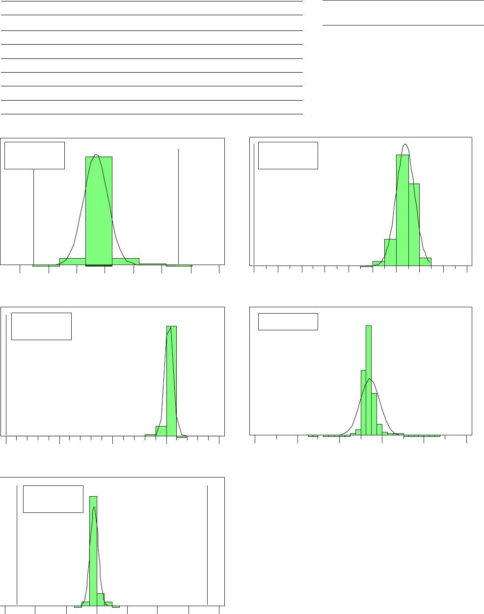
.36 .38 .4 .42 .44 .46 .48 .5
CPK = 1.26
Std Dev = 10.6
44.5 45 45.5 46 46.5 47 47.5 48 48.5 49
CPK = 4.51
Std Dev = 0.254
30 30.5 31 31.5 32
CPK = 12.1
Std Dev = 0.042
50 51 52 53 54 55
Std Dev = 0.254
1
3.5 14 14.5 15 15.5 16 16.5 17
CPK = 5.0
Std Dev = 0.085
Absolute Maximum Rating
[2]
T
A
=25°C
Symbol Parameter Units Absolute Max.
V
dd, max
Device Voltage, RF output to ground V 5.5
I
ds, max
Device Drain Current mA 750
V
ctrl,max
Control Voltage V 5.5
P
in,max
CW RF Input Power dBm 25
P
diss
Total Power Dissipation
[4]
W 4.125
T
j,max
Junction Temperature
o
C 150
T
STG
Storage Temperature
o
C -65 to 150
Product Consistency Distribution Charts
[5, 6]
Thermal Resistance
[3]
θ
jc
= 25 °C/W
(Vdd = 5V, Idd = 400mA, Tc = 85 °C)
Notes:
2. Operation of this device in excess of any of
these limits may cause permanent damage.
3. Thermal resistance measured using Infra-Red
measurement technique.
4. This is limited by maximum Vdd and Ids.
Derate 40mW/ °C for T
C
>46.9 °C.
Figure 1: Ids; LSL = 370mA, nominal = 415mA, USL = 470mA
Figure 2: OIP3; LSL = 44.5dBm, nominal = 47.9dBm
Figure 3: P1dB; LSL = 30dBm, nominal = 31.5dBm
Figure 4: PAE at P1dB; nominal = 52.6%
Figure 5: Gain; LSL=13.7dB, Nominal = 14.9dB, USL=16.8dB
Notes:
5. Distribution data sample size is 500 samples taken from 2 dierent
wafers lots. T
A
= 25°C, Vdd = 5V, Vctrl = 5V, RF performance at 2GHz
unless otherwise specied. Future wafers allocated to this product
may have nominal values anywhere between the upper and lower
limits.
6. Measurements are made on a production test board. Input trace
losses have not been de-embedded from actual measurements.
3
Electrical Specications
[7]
T
A
= 25 °C, Vdd =5V, Vctrl=5V, RF performance at 2.0 GHz, measured on demo board (see Figure 7) unless otherwise
specied.
Symbol Parameter and Test Condition Units Min. Typ. Max.
Ids Quiescent current mA 370 415 470
Ictrl Vctrl current mA - 10.4 -
Gain Gain dB 13.7 14.9 16.8
OIP3
[8]
Output Third Order Intercept Point dBm 44.5 47.9 -
OP1dB Output Power at 1dB Gain Compression dBm 30 31.5 -
PAE Power Added Eciency % - 52 -
NF Noise Figure dB - 2.7 -
S11 Input Return Loss, 50Ω source dB - -10 -
S22 Output Return Loss, 50Ω load dB - -10 -
S12 Reverse Isolation dB - -30 -
Notes:
7. Measurements at 2GHz obtained using demo board described in Figure 6 and 7.
8. 2GHz OIP3 test condition: F
RF1
- F
RF2
= 10MHz with input power of -5dBm per tone measured at worse case side band.
9. Use proper bias, heat sink and de-rating to ensure maximum channel temperature is not exceeded. See absolute maximum ratings and
application note (if applicable) for more details.

ALM-31222-TR2G

Mfr. #:
Manufacturer:
Broadcom / Avago
Description:
RF Amplifier Meranti 1W 2GHz
Lifecycle:
New from this manufacturer.
Delivery:
DHL FedEx Ups TNT EMS
Payment:
T/T Paypal Visa MoneyGram Western Union

Products related to this Datasheet