IRFR/U540ZPbF
2 www.irf.com
S
D
G
Electr
cal
haracter
st
cs
T
J
= 25°
unless otherw
se spec
ed
Parameter Min. Typ. Max. Units
V
(BR)DSS
Drain-to-Source Breakdown Voltage 100 ––– ––– V
∆
V
(BR)DSS
/
∆
T
J
Breakdown Voltage Temp. Coefficient ––– 0.092 ––– V/°C
R
DS(on)
Static Drain-to-Source On-Resistance ––– 22.5 28.5
mΩ
V
GS(th)
Gate Threshold Voltage 2.0 ––– 4.0 V
gfs Forward Transconductance 28 ––– ––– S
I
DSS
Drain-to-Source Leakage Current ––– ––– 20 µA
––– ––– 250
I
GSS
Gate-to-Source Forward Leakage ––– ––– 200 nA
Gate-to-Source Reverse Leakage ––– ––– -200
Q
g
Total Gate Charge ––– 39 59
Q
gs
Gate-to-Source Charge ––– 11 ––– nC
Q
gd
Gate-to-Drain ("Miller") Charge ––– 12 –––
t
d(on)
Turn-On Delay Time ––– 14 –––
t
r
Rise Time ––– 42 –––
t
d(off)
Turn-Off Delay Time ––– 43 ––– ns
t
f
Fall Time ––– 34 –––
L
D
Internal Drain Inductance ––– 4.5 ––– Between lead,
nH 6mm (0.25in.)
L
S
Internal Source Inductance ––– 7.5 ––– from package
and center of die contact
C
iss
Input Capacitance ––– 1690 –––
C
oss
Output Capacitance ––– 180 –––
C
rss
Reverse Transfer Capacitance ––– 100 ––– pF
C
oss
Output Capacitance ––– 720 –––
C
oss
Output Capacitance ––– 110 –––
C
oss
eff. Effective Output Capacitance ––– 190 –––
Source-Drain Ratin
s and Characteristics
Parameter Min. Typ. Max. Units
I
S
Continuous Source Current ––– ––– 35
(Body Diode) A
I
SM
Pulsed Source Current ––– ––– 140
(Body Diode)
V
SD
Diode Forward Voltage ––– ––– 1.3 V
t
rr
Reverse Recovery Time ––– 32 48 ns
Q
rr
Reverse Recovery Charge ––– 40 60 nC
t
on
Forward Turn-On Time Intrinsic turn-on time is negligible (turn-on is dominated by LS+LD)
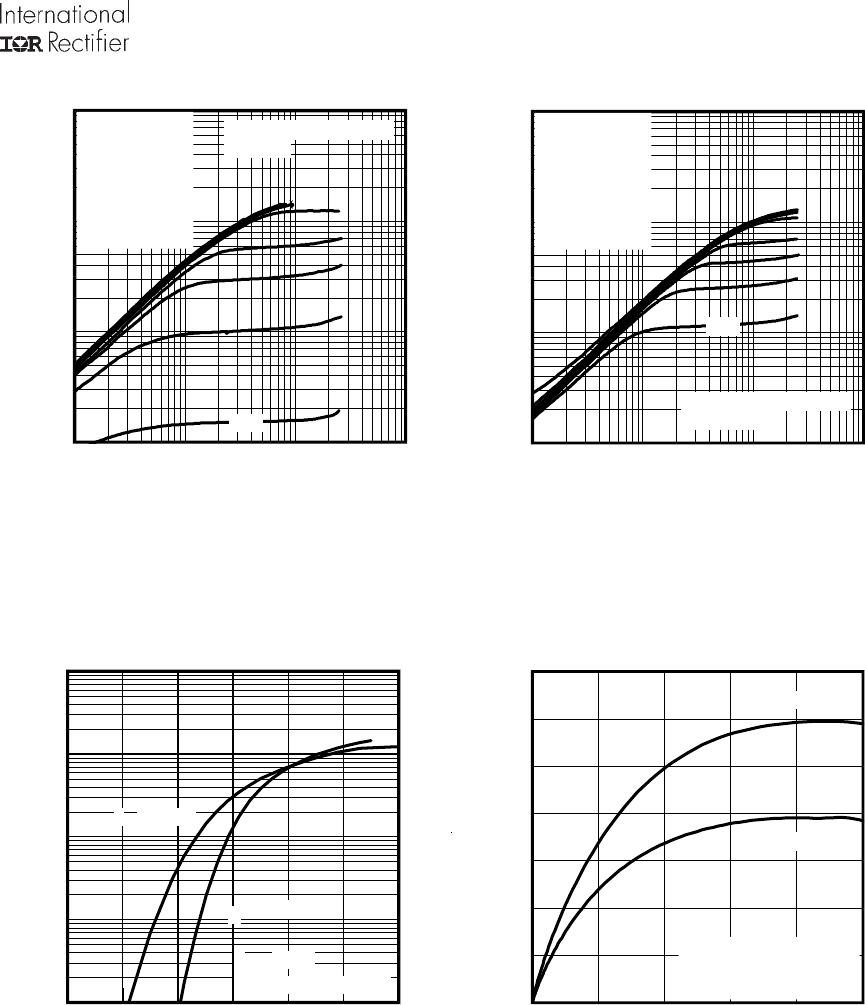
V
GS
= 10V
V
DD
= 50V
I
D
= 21A
R
G
= 13 Ω
T
J
= 25°C, I
S
= 21A, V
GS
= 0V
T
J
= 25°C, I
F
= 21A, V
DD
= 50V
di/dt = 100A/µs
Conditions
V
GS
= 0V, I
D
= 250µA
Reference to 25°C, I
D
= 1mA
V
GS
= 10V, I
D
= 21A
V
DS
= V
GS
, I
D
= 50µA
V
DS
= 100V, V
GS
= 0V
V
DS
= 100V, V
GS
= 0V, T
J
= 125°C
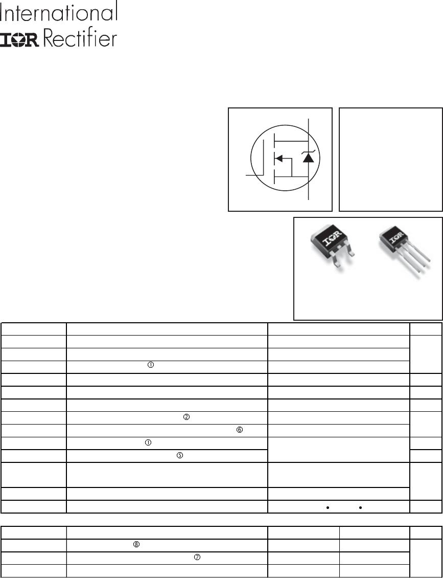
MOSFET symbol
showing the
integral reverse
p-n junction diode.
Conditions
V
GS
= 10V
V
GS
= 0V
V
DS
= 25V
ƒ = 1.0MHz
V
GS
= 0V, V
DS
= 1.0V, ƒ = 1.0MHz
V
GS
= 0V, V
DS
= 80V, ƒ = 1.0MHz
V
GS
= 0V, V
DS
= 0V to 80V
V
GS
= 20V
V
GS
= -20V
V
DS
= 50V
V
DS
= 25V, I
D
= 21A
I
D
= 21A