MAX2611EUS+T

MAX2611
DC-to-Microwave, Low-Noise Amplifier
4 _______________________________________________________________________________________
______________________________________________________________Pin Description
NAME FUNCTION
1 OUT
Amplifier Output. Use a series blocking capacitor with less than 3 reactance at your lowest operat-
ing frequency. Bias with an external resistor and an optional RF choke.
2, 4 GND
Ground Connection. For optimum performance, provide a low-inductance connection to the ground
plane.
PIN
3 IN
Amplifier Input. Use a series blocking capacitor with less than 3 reactance at your lowest operating
frequency.
Table 1. Typical Scattering Parameters
(I
D
= 16mA, Z
0
= 50, T
A
= +25°C)
3.0
0.3
0.2
0.1
2.5
2.0
1.5
1.0
0.4
0.5
0.6
0.8
FREQUENCY
(GHz)
0.20
0.32
0.31
0.32
0.12
0.13
0.15
0.15
0.14
0.13
0.11
0.12
S11
(mag)
-70
-76
-72
-60
16
50
77
-89
-78
-58
-44
-11
S11
(ang)
5.9
7.9
10.3
14.1
16.6
17.4
18.1
18.3
18.5
18.6
18.8
19.0
S21
(dB)
1.98
2.48
3.27
5.07
6.79
7.45
7.99
8.26
8.43
8.53
8.73
8.90
S21
(mag)
32
47
59
79
109
123
137
144
151
158
166
173
S21
(ang)
-22.3
-22.6
-22.2
-21.8
-20.9
-21.6
-21.6
-21.6
-21.6
-21.6
-21.9
-22.6
S12
(dB)
0.077
0.074
0.078
0.081
0.090
0.083
0.083
0.083
0.083
0.083
0.081
0.074
S12
(mag)
37
25
18
11
10
10
9
7
6
5
4
2
S12
(ang)
0.24
0.26
0.22
0.21
0.10
0.10
0.09
0.08
0.06
0.04
0.03
0.05
S22
(mag)
-29
-53
-72
-86
35
23
26
34
32
45
12
53
S22
(ang)
3.10
2.44
1.87
1.29
1.11
1.10
1.07
1.06
1.06
1.05
1.06
1.08
K
3.5 0.24 -64 3.0 1.41 13 -21.4 0.086 30 0.19 47 3.83
4.0
0.31 -68 -0.7 0.92 17 -23.0 0.070 35 0.24 82 6.66
MAX2611
DC-to-Microwave, Low-Noise Amplifier
_______________________________________________________________________________________ 5
_______________Detailed Description
The MAX2611 is a broadband amplifier with flat gain
and 50 input and output ports. Its small size and sim-
ple bias circuitry make it ideal for applications where
board space is limited.
__________Applications Information
External Components
As shown in the Typical Operating Circuit, the
MAX2611 is easy to use. Input and output series
capacitors may be necessary to block DC bias volt-
ages (generated by the MAX2611) from interacting with
adjacent circuitry. These capacitors must be large
enough to contribute negligible reactance in a 50
system at the minimum operating frequency. Use the
following equation to calculate their minimum value:
where f (in MHz) is the minimum operating frequency.
Bias current is supplied to the MAX2611 through an
external resistor and optional RF choke connected
between V
CC
and the OUT pin. A bypass capacitor
from V
CC
to GND may be necessary to isolate the V
CC
line from other circuitry. The resistor value determines
the bias current from the following equation:
where V
D
is the device voltage, nominally 3.8V.
An optional RF choke can be added to improve the
MAX2611’s gain and output power. The choke should
be large enough to reduce the loading effect that the
bias resistor has on the amplifier output. This is a func-
tion of R
BIAS
, frequency of operation, and output
impedance.
Grounding
Proper grounding of the GND pins is essential. If the
PC board uses a topside RF ground, the GND pins
should be connected directly to it. For a board where
the ground plane is not on the component side, the
best technique is to connect the GND pins to it through
multiple plated through-holes.
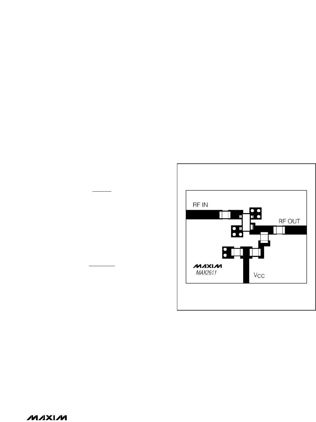
PC Board Layout Example
An example PC board layout is given in Figure 1. It
uses FR-4 with 31mil layer thickness between the RF
lines and the ground plane. This board satisfies all the
above requirements.
I
D
=
V
CC
- V
D
R
BIAS
C
BLOCK
=
53,000
f
(pF)
Figure 1. Example PC Board Layout
EXPANDED VIEW
Maxim cannot assume responsibility for use of any circuitry other than circuitry entirely embodied in a Maxim product. No circuit patent licenses are
implied. Maxim reserves the right to change the circuitry and specifications without notice at any time.
6 ___________________Maxim Integrated Products, 120 San Gabriel Drive, Sunnyvale, CA 94086 (408) 737-7600
© 2005 Maxim Integrated Products Printed USA is a registered trademark of Maxim Integrated Products, Inc.
MAX2611
DC-to-Microwave, Low-Noise Amplifier
SOT-143 4L.EPS
E
1
1
21-0052
PACKAGE OUTLINE, SOT-143, 4L
4.0 ±0.1
0.30 ±0.05
0.8 ±0.05
0.30R MAX.
B
o
Ko
2.2 ±0.1
0.5 RADIUS
TYPICAL
A0
4.0 ±0.1
2.0 ±0.05
1.5 +0.1/-0.0 DIAMETER
1.75 ±0.1
1.0 ±0.1
A
8.0 ±0.3
3.5 ±0.05
1.0 MINIMUM
A
DF = MAX2611
Ao = 3.1mm ±0.1
Bo = 2.7mm ±0.1
Ko = 1.2mm ±0.1
X X X X
LOT SPECIFIC
CODE
MARKING
INFORMATION
NOTE: DIMENSIONS ARE IN MM.
AND FOLLOW EIA481-1 STANDARD.
ICs MAY ALSO BE MARKED WITH FULL PART NAME: 2611
__________________________________________________Tape-and-Reel Information
Package Information
(The package drawing(s) in this data sheet may not reflect the most current specifications. For the latest package outline information,
go to www.maxim-ic.com/packages
.)

MAX2611EUS+T

Mfr. #:
Manufacturer:
Maxim Integrated
Description:
RF Amplifier DC-to-Microwave Amplifier
Lifecycle:
New from this manufacturer.
Delivery:
DHL FedEx Ups TNT EMS
Payment:
T/T Paypal Visa MoneyGram Western Union

Products related to this Datasheet